






Typical Specification Range
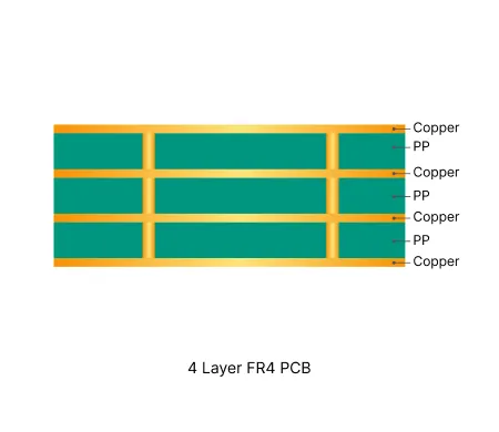
| Parameter | Typical Range |
|---|---|
| Layer count | 4 layers |
| Material type | FR4 TG130 to TG170 |
| Surface finish | HASL, ENIG, OSP |
| Thickness | 0.8mm – 1.6mm |
| Solder mask | Green, black, red, white, yellow, blue, purple, matte black |
| Copper thickness | 1oz – 8oz |
| Special features | Impedance control, via plugging, heavy copper, gold fingers |
Manufacturing Process Insights
Inner Layer Imaging & Etching Inner cores are imaged and etched first. Precise registration and etch-factor control are essential to maintain annular rings and impedance on signal layers.
Lamination & Stackup Control Cores and prepregs are stacked and laminated under heat and pressure. Copper balance and dielectric thickness uniformity are critical to control warpage and registration on 4-layer boards, especially thin (1.0–1.2 mm) constructions.
Precision Drilling CNC drilling creates through-holes (and any blind vias). Parameters are optimized for layer-to-layer registration and hole-wall quality, particularly on high-aspect-ratio or mixed-copper designs.
Desmear & Electroless Copper Resin smear is removed and electroless copper deposited. Uniform coverage ensures reliable plating of through-holes and any controlled-depth features.
Pattern Plating & Outer Layer Etching Outer layers are imaged, plated and etched. Tight registration to inner layers and controlled etch compensation prevent undercut and maintain fine-line integrity.
Solder Mask Application Liquid photoimageable mask is applied and developed. Via tenting/plugging decisions and mask openings on gold fingers or dense areas are finalized here to avoid ink intrusion and exposed copper.
Surface Finish HASL, ENIG or OSP is applied according to assembly needs. Process control ensures uniform coverage on both outer pads and plated through-holes while preserving dimensional stability.
Routing, V-Scoring & Depanelization Boards are separated by routing, V-scoring or both. Tab strength, stamp-hole design, copper-to-edge clearance and fiducial protection are verified to prevent edge defects on multilayer panels.
Electrical Test & Final Inspection 100% flying-probe or fixture testing confirms continuity and isolation across all layers. Final inspection against IPC criteria (edge condition, registration, solder-mask quality) ensures only compliant boards are shipped.
Manufacturing Order Profile
| Order Quantity | Order Proportion | Estimated Price Level | Typical Lead Time |
|---|---|---|---|
| Prototype (<=30 pcs) | 55% | From $1 | From 2 days |
| Small volume (30-200 pcs) | 30% | From $70 | From 2 days |
| Mass production (>200 pcs) | 15% | From $140 | From 3 days |
Manufacturing Challenges & Process Optimization
Stackup Confirmation & Thickness Control on Thin 4-Layer Boards
Customer-provided stackup diagrams frequently mismatch available copper-clad cores or target finished thickness (especially 1.0–1.2 mm).
Uneven copper distribution or incorrect prepreg selection leads to warpage, registration shift and thickness deviation outside tolerance.
On thin 4-layer constructions these variations directly affect impedance stability and mechanical reliability.
✓ Confirm and adjust stackup to proven copper-clad cores while holding target thickness.
✓ Verify copper balance and dielectric symmetry before lamination.
✓ Apply enhanced press monitoring for thin panels to stay within ±0.10–0.12 mm capability.
Design Considerations
Provide a complete stackup diagram that matches available core and prepreg materials. For thin 4-layer boards (1.0–1.2 mm), design symmetrical copper distribution and confirm finished thickness tolerance early to control warpage and registration.
Account for etch factor and layer-to-layer registration on inner cores. Avoid extreme copper imbalance between layers. Clearly define any controlled-impedance traces and associated dielectric requirements.
Fully specify gold-finger bevel and solder-mask openings on both sides. Document any blind or controlled-depth drilling requirements with clear depth targets. Size non-plated slots with routing tolerance in mind and explicitly state via plugging method.
Design stamp holes and breakaway tabs with adequate strength for thin multilayer panels. Always protect process-edge fiducials with copper rings. Consider process-edge copper pour to improve plating uniformity and reduce warpage risk.