

Typical Specification Range

Parameter Typical Range
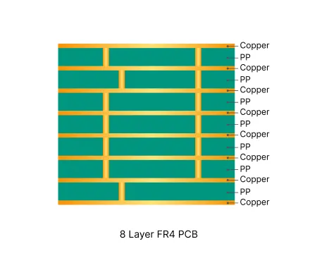
Layer count 8 layers
Material type FR4, High Tg FR4
Surface finish ENIG, HASL, Immersion Silver
Thickness 1.0mm to 3.0mm
Solder mask Green, black, red, white, yellow, blue, purple, matte black
Copper thickness 1oz to 2oz
Special features Impedance control, blind vias, buried vias

Manufacturing Process Insights

Lamination: Manufacturing 8-layer FR4 PCBs involves greater complexity than lower layer count boards due to multiple lamination cycles, the integration of blind and buried vias, and stricter requirements for dimensional stability and electrical performance. Based on our production experience, several process stages require focused control to ensure consistent quality and yield. Multi-stage Lamination 8-layer boards are typically built using two or three lamination cycles, depending on the stackup design. Each lamination introduces risks related to layer registration, resin flow, and thermal stress. We pay close attention to temperature ramp rates, pressure distribution, and vacuum levels during pressing to minimize voids and delamination. Symmetric copper distribution across the stackup, combined with copper thieving patterns, is applied to reduce warpage caused by repeated thermal cycles.

Drilling: Drilling and Via Processing Drilling operations in 8-layer boards include through holes, blind vias, and buried vias. Blind and buried vias require more precise depth control and specialized desmear processes, particularly when high Tg materials are used. We implement staged drilling strategies and optimize parameters according to via type and material characteristics to maintain hole wall quality and ensure reliable plating adhesion.

Plating: Plating and Metallization Higher layer counts result in increased aspect ratios, making uniform copper deposition inside vias more challenging. Our process focuses on controlling both electroless and electrolytic plating steps to achieve consistent barrel thickness. Regular cross-section analysis is performed to verify plating quality, especially for blind and buried vias where plating defects can be difficult to detect through standard electrical testing.

Surface Finish: Surface Finish Selection and Application ENIG is the predominant surface finish for 8-layer FR4 boards, especially when fine-pitch components or BGAs are present. We adjust nickel and gold thickness based on copper weight, assembly requirements, and shelf-life expectations. For boards with higher copper weights or specific thermal demands, alternative finishes such as Immersion Silver or HASL may be recommended after evaluating solderability and long-term reliability needs.

Manufacturing Order Profile

Order Quantity Order Proportion Estimated Price Level Typical Lead Time
Prototype (<=30 pcs) 61% From $110 From 4 days
Small volume (30-200 pcs) 26% From $130 From 5 days
Mass production (>200 pcs) 13% From $200 From 6 days

Manufacturing Challenges & Process Optimization

Challenge: Layer Registration Control
Multiple lamination cycles increase the difficulty of maintaining accurate layer-to-layer alignment. Misregistration can lead to reduced annular rings, particularly around blind and buried vias, which may compromise via reliability under thermal stress.

We prioritize symmetric stackup designs and apply copper thieving patterns to balance copper distribution across layers. Pinned lamination fixtures and X-ray alignment systems are used to improve registration accuracy. After lamination, X-ray inspection and cross-section analysis are conducted to verify alignment before drilling. These measures have been particularly effective in boards with dense blind via structures.

Design Considerations

Symmetric Stackup Design

Maintaining symmetry in the layer stackup is one of the most effective ways to control warpage in multi-lamination boards. Placing critical signal layers adjacent to reference planes also supports better impedance control and electromagnetic performance. Early definition of a balanced stackup helps minimize issues during subsequent lamination cycles.

Blind and Buried Via Strategy

The placement and depth of blind and buried vias should be carefully planned to avoid excessive process complexity. Avoiding the positioning of dense routing or large copper areas directly beneath blind via fields can reduce registration risks. Clear via definitions in the design data also help prevent ambiguity during engineering review.

Copper Distribution Balance

Uneven copper density across layers or within individual layers can affect lamination quality and final board dimensions. Designers are encouraged to apply copper thieving or grid patterns in areas with low copper density. This practice improves pressure distribution during lamination and reduces the likelihood of localized stress or warpage.

Impedance Control and Trace Routing

For designs requiring controlled impedance, it is important to define target values and reference layers early. Routing impedance traces with minimal interruptions from vias or irregular copper pours helps maintain consistency. Providing sufficient space for trace width adjustments during the engineering phase can prevent delays in production release.

Get in Touch


    Typical Specification Range
    Parameter Typical Range
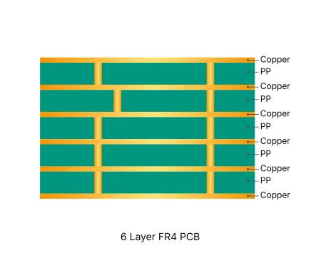
    Layer count 6 layers
    Material type FR4 TG130 to TG170
    Surface finish ENIG, HASL, OSP
    Thickness 0.8 mm to 3.0 mm
    Solder mask Green, black, red, white, yellow, blue, purple, matte black
    Copper thickness 1 oz to 4 oz
    Special features Impedance control, blind vias, buried vias, via-in-pad

    Manufacturing Process Insights

    Inner Layer Imaging & Etching Multiple cores are imaged and etched with high registration accuracy. Precise annular-ring control and etch-factor compensation on inner layers are essential to maintain impedance and via reliability across the six-layer structure.

    Lamination & Stackup Control Cores and prepregs are stacked in a controlled sequence and laminated under heat and pressure. Symmetric copper distribution and dielectric thickness uniformity across all six layers are critical to minimize warpage, ensure layer-to-layer registration, and achieve consistent impedance.

    Precision Drilling CNC drilling creates through-holes (and any controlled-depth features) with tight positional tolerance. Higher aspect ratios in 6-layer boards require optimized drill parameters to control hole-wall quality and registration to inner-layer pads.

    Desmear & Plating Resin smear is thoroughly removed and electroless copper is deposited, followed by electrolytic plating. Uniform barrel plating through the full board thickness is vital for via reliability under thermal cycling.

    Outer Layer Patterning & Etching Outer layers are imaged, plated and etched. Trace compensation and reference-plane integrity are verified to meet controlled-impedance targets common on 6-layer designs.

    Solder Mask & Via Treatment Solder mask is applied with accurate registration. Via tenting, resin plugging or open-window decisions are finalized here; conflicts between plugging and mask openings are resolved to protect surface planarity and solderability.

    Routing, V-Scoring & Final Inspection Boards are separated by routing or V-scoring. Edge clearance, panelization integrity and copper-to-outline spacing are confirmed. 100% electrical testing and dimensional inspection ensure multilayer continuity and compliance before shipment.

    Manufacturing Order Profile

    Order Quantity Order Proportion Estimated Price Level Typical Lead Time
    Prototype (<=30 pcs) 58% From $30 From 2 days
    Small volume (30-200 pcs) 27% From $80 From 2 days
    Mass production (>200 pcs) 15% From $140 From 3 days

    Manufacturing Challenges & Process Optimization

    Stackup Confirmation & Copper Balance / Warpage Control
    Customer-supplied stackups frequently deviate from proven 6-layer constructions, creating asymmetric copper distribution or incorrect dielectric thicknesses.
    This leads to warpage, registration shift, thickness deviation and unstable impedance — problems that are significantly amplified compared with 2- or 4-layer boards.

    ✓ Align stackup to a symmetric, process-proven 6-layer configuration while preserving target thickness and impedance.
    ✓ Enforce balanced copper distribution across all layers.
    ✓ Verify finished thickness and bow/twist against IPC limits after first-article lamination.

    Design Considerations

    Stackup & Copper Balance

    Provide a complete, symmetric stackup that matches available core and prepreg materials for 6-layer FR4. Design balanced copper distribution across all layers to control warpage and registration. Confirm finished thickness tolerance early, especially for 1.6 mm or thinner constructions.

    Impedance & Reference Planes

    Define controlled-impedance requirements with clear stackup and trace geometry. Ensure continuous reference planes (or adequate copper pour/stitching) under impedance-critical traces. Size traces according to actual copper weight and expected etch compensation rather than theoretical values.

    Hole Attribute Clarity

    Explicitly annotate every hole as PTH or NPTH in both the drill file and fabrication notes. When NPTH holes carry surface pads for mechanical support, state this intent clearly so plating sequence can be set correctly. Avoid hybrid features that create plating ambiguity.

    Via Treatment Consistency

    Specify via plugging or tenting method for every via group and ensure the solder-mask openings match that treatment exactly. Avoid single-sided openings on resin-plugged vias. Keep silkscreen clear of plugged via areas to prevent resin overflow and planarity problems.

    Get in Touch


      Typical Specification Range

      Parameter Typical Range
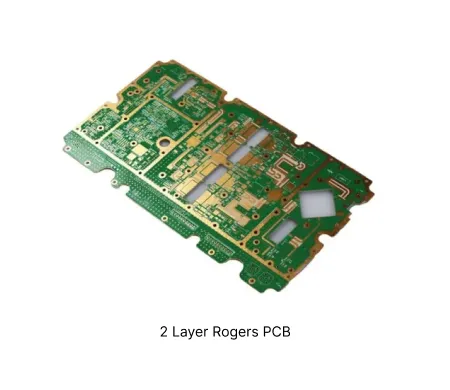
      Layer count 2 layers
      Material type Rogers RO4350B, RO4003C, RT/duroid 5880
      Surface finish ENIG, Immersion Silver, OSP
      Thickness 0.101mm to 0.762mm
      Solder mask Green, Black, Blue
      Copper thickness 0.5oz to 2oz
      Special features Controlled impedance, low loss tangent, precise registration

      Manufacturing Process Insights

      Lamination
      Rogers core is bonded with copper foil under tightly controlled temperature and pressure.

      Drilling
      Specialized parameters and tools minimize smear on PTFE substrates. Plasma desmear follows to clean hole walls.

      Plating
      Electroless copper seed layer enables reliable via metallization before pattern plating.

      Surface Finish Logic
      ENIG is selected to maintain smooth surface for RF performance while ensuring assembly compatibility.

      Risk Control
      In-process impedance testing and cross-section verification prevent field failures.

      Manufacturing Order Profile

      Order Quantity Order Proportion Estimated Price Level Typical Lead Time
      Prototype (<=30 pcs) 65% From $140 From 7 days
      Small volume (30-200 pcs) 25% From $150 From 8 days
      Mass production (>200 pcs) 10% From $300 From 10 days

      Manufacturing Challenges & Process Optimization

      PTFE Drilling Smear
      Mechanical drilling of Rogers PTFE materials frequently leaves residue on via barrel walls.
      Material softness and high melting point prevent clean cutting and promote heat-induced smearing.
      Residue blocks electroless copper adhesion causing plating voids. This reduces yield and creates intermittent via failures under thermal stress.

      Utilize peck drilling cycles with specialized bits and reduced feed rates.
      Apply plasma desmear process optimized for fluoropolymer substrates.
      Validate plating integrity through cross-section analysis and IST testing.

      Design Considerations

      Stackup Design

      Core thickness selection determines impedance value. Copper roughness must be factored into calculations. Balanced construction minimizes board bow.

      Via Strategy

      Through vias are standard for 2 layer boards. Backdrilling reduces stub effects at microwave frequencies. Avoid unnecessary blind vias due to added cost.

      Material Selection

      Match DK and dissipation factor to operating frequency. RO4350B balances performance with processability. Verify material availability against production volume.

      Surface Finish

      ENIG provides flat surface required for RF signals. Avoid HASL due to uneven topography. Gold thickness affects both solderability and long term oxidation resistance.

      Get in Touch


        Typical Specification Range

        Parameter Typical Range
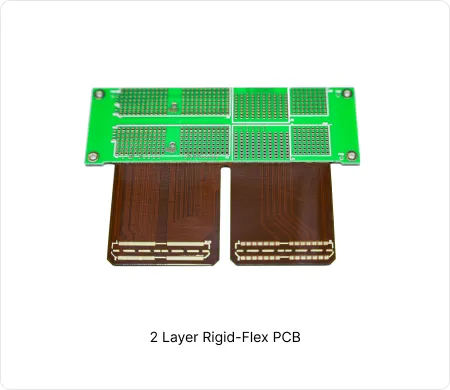
        Layer count 2 layers
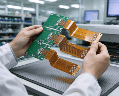
        Material type Polyimide flex with selective FR4 rigid laminations
        Surface finish ENIG, OSP, Immersion Silver
        Thickness Rigid board thickness 0.3mm – 1.6mm, FPC Thickness 0.08mm – 0.2mm
        Solder mask Flexible solder mask and polyimide coverlay
        Copper thickness 0.5oz to 2oz
        Special features Selective bonding, stiffeners, controlled bend areas, ZIF fingers

        Manufacturing Process Insights

        Lamination: FR4 rigid material is selectively bonded to polyimide flex core using no-flow prepreg. Precise registration and controlled pressure prevent wrinkles at transition zones.

        Drilling and Plating: Mechanical drilling creates vias. Chemical copper deposition followed by electrolytic plating establishes interlayer connections. Plasma treatment improves hole wall adhesion.

        Surface Finish and Coverlay: ENIG is applied for solderability. Polyimide coverlay protects flex circuits. Strict process sequencing minimizes thermal stress on flex material.

        Risk Control: Cross-section inspection verifies bonding quality. CTE mismatch is managed through material selection and lamination profiles.

        Manufacturing Order Profile

        Order Quantity Order Proportion Estimated Price Level Typical Lead Time
        Prototype (<=30 pcs) 66% From $215 From 13 days
        Small volume (30-200 pcs) 19% From $315 From 15 days
        Mass production (>200 pcs) 15% From $649 From 16 days

        Manufacturing Challenges & Process Optimization

        Transition Zone Delamination
        Delamination occurs at rigid-flex junctions during thermal cycling or assembly.
        CTE mismatch between FR4 and polyimide with insufficient resin flow creates weak bonds.
        This defect lowers yield and causes intermittent opens that reduce product reliability.

        Use stepped lamination with optimized pressure and temperature profiles.
        Apply plasma treatment to flex surfaces before bonding.
        Perform cross-section analysis on first articles to verify interface integrity.

        Design Considerations

        Stackup Design

        Define clear rigid and flex zones in planning. Maintain uniform dielectric thickness for impedance control. Minimize transition steps to improve manufacturability and reduce stress concentration.

        Via Strategy

        Place plated through holes only in rigid sections. Avoid vias in flex bend areas. This reduces production risk and prevents copper cracking during repeated flexing.

        Material Selection

        Choose adhesive-less polyimide for improved flexibility and thermal performance. Balance bend endurance with cost. Material selection affects long-term reliability under thermal and mechanical stress.

        Surface Finish

        ENIG offers excellent solderability for mixed assembly. It provides oxidation protection on exposed copper. This finish supports reliable multiple reflow cycles in production.

        Get in Touch


          Typical Specification Range

          Parameter Typical Range
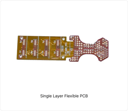
          Layer count 1
          Material type Polyimide film, PET film
          Surface finish ENIG, OSP, Immersion tin
          Thickness 0.1mm – 0.32mm
          Solder mask Yellow, white, black
          Copper thickness 0.5oz to 1oz
          Special features Dynamic flex capability, stiffener attachment, tight bend radius

          Manufacturing Process Insights

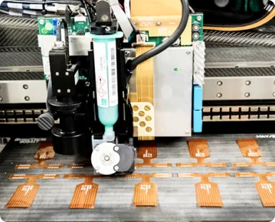
          Lamination bonds copper foil to dielectric film under controlled heat and tension.

          Patterning applies photoresist, exposes, develops, then etches copper traces.

          Drilling or punching creates component holes with precise registration.

          Plating deposits metal in holes when electrical continuity is required.

          Surface finish is applied according to assembly method and storage duration.

          Risk control centers on material shrinkage management and registration accuracy throughout all thermal steps.

          Manufacturing Order Profile

          Order Quantity Order Proportion Estimated Price Level Typical Lead Time
          Prototype (<=30 pcs) 54% From $43 From 4 days
          Small volume (30-200 pcs) 34% From $70 From 4 days
          Mass production (>200 pcs) 12% From $139 From 5 days

          Manufacturing Challenges & Process Optimization

          Material Shrinkage During Processing
          Single layer flex films exhibit dimensional change when exposed to repeated thermal cycles.
          High CTE of polyimide and built-in copper stress create unpredictable movement across panels.
          Dimensional variation causes registration errors that reduce yield and prevent consistent final form factor.

          Apply stabilized pre-baking and tension control prior to lamination.
          Use vacuum fixtures and laser fiducial systems to maintain alignment during pressing.
          Conduct automated optical inspection after each critical thermal process step.

          Design Considerations

          Stackup Design

          Single layer stackups define copper position relative to bend axis. Coverlay thickness and adhesive flow must be considered. Stiffener locations require careful planning for mechanical support.

          Via Strategy

          Vias are minimized on single layer flex to preserve flexibility. When required, larger hole diameters improve plating reliability. Plated holes increase cracking risk during repeated bending.

          Material Selection

          Polyimide provides higher temperature rating than PET. Adhesiveless constructions offer better dimensional stability. Material choice balances flexibility, cost, and environmental resistance.

          Surface Finish

          ENIG suits most soldering applications on flex circuits. OSP reduces cost but limits shelf life. Finish selection must match assembly process and operating environment.

          Get in Touch


            Typical Specification Range

            Parameter Typical Range
            Layer count 1
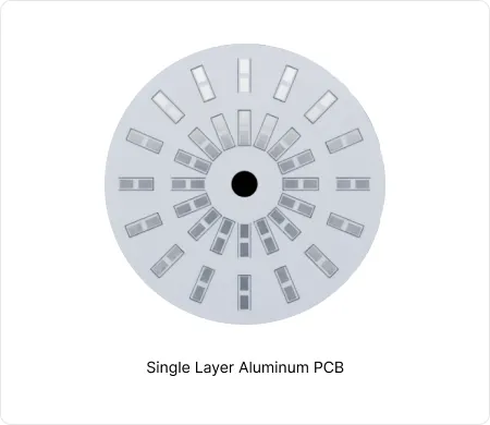
            Material type Aluminum alloy base with dielectric layer
            Surface finish HASL, ENIG, OSP
            Thickness 0.8mm to 3.2mm
            Solder mask White, Black
            Copper thickness 1oz to 2oz
            Special features High thermal conductivity, exposed aluminum options, selective plating

            Manufacturing Process Insights

            Material Preparation and Lamination
            Aluminum sheets are cleaned then bonded with dielectric film and copper foil under controlled heat and pressure.

            Patterning and Etching
            Photoresist application, exposure, and etching define the circuit pattern on the copper layer.

            Drilling and Plating
            Precision drilling creates holes. Copper plating follows to establish electrical connections where required.

            Surface Finish Application
            Finish selection balances solderability, thermal performance, and environmental protection needs.

            Process controls manage thermal expansion mismatch to prevent warping during lamination and assembly.

            Manufacturing Order Profile

            Order Quantity Order Proportion Estimated Price Level Typical Lead Time
            Prototype (<=30 pcs) 44% From $1 From 1 day
            Small volume (30-200 pcs) 28% From $5 From 1 day
            Mass production (>200 pcs) 28% From $40 From 1 day

            Manufacturing Challenges & Process Optimization

            Warpage During Lamination
            Single layer aluminum PCBs tend to warp when subjected to repeated thermal cycles during manufacturing and assembly.
            Root cause relates to the mismatch in thermal expansion coefficients between the aluminum base and copper foil under heat and pressure.
            Warpage reduces SMT placement accuracy, creates inconsistent solder joints, and lowers long-term reliability in power electronics.

            Optimized lamination parameters reduce internal stress.
            Engineers apply controlled ramp rates and balanced pressure profiles. Preconditioning of raw materials removes moisture before bonding.
            Flatness inspection under thermal stress verifies compliance before release to assembly.

            Design Considerations

            Stackup Design

            Define stackup with appropriate dielectric thickness between aluminum base and copper. This controls thermal resistance and electrical isolation. Account for final thickness effects on mechanical stability during reflow.

            Via Strategy

            Limit plated through vias due to the conductive aluminum core. Surface mount technology is preferred. Thermal relief strategies must maintain electrical isolation while supporting heat flow.

            Material Selection

            Select aluminum alloy according to thermal conductivity and mechanical strength needs. Dielectric choices balance heat transfer with processability. Verify material compatibility with operating environment and assembly temperatures.

            Surface Finish

            Match surface finish to assembly process and product lifecycle. ENIG offers reliable soldering and corrosion resistance. OSP suits cost-driven applications with controlled storage and shorter service life.

            Get in Touch


              Typical Specification Range

              Parameter Typical Range
              Layer count 4 layers
              Material type FR-4, High Tg FR-4
              Surface finish ENIG, OSP, Immersion Tin
              Thickness 0.4mm to 3.2mm
              Solder mask Green, black, red, white, yellow, blue, purple
              Copper thickness 0.5oz to 2oz
              Special features Blind microvias, stacked vias, fine pitch lines

              Manufacturing Process Insights

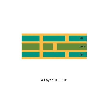
              Sequential Lamination: Inner core is laminated first. Outer layers add through controlled press cycles with prepreg.

              Laser Drilling: UV and CO2 lasers create microvias. Plasma desmear follows to clean via walls.

              Plating Logic: Direct metallization and electrolytic copper fill microvias uniformly. Current density is tightly controlled.

              Surface Finish: ENIG is preferred for fine pitch assembly reliability.

              Registration control and via inspection mitigate risks throughout the process.

              Manufacturing Order Profile

              Order Quantity Order Proportion Estimated Price Level Typical Lead Time
              Prototype (<=30 pcs) 69% From $180 From 7 days
              Small volume (30-200 pcs) 22% From $220 From 8 days
              Mass production (>200 pcs) 9% From $330 From 8 days

              Manufacturing Challenges & Process Optimization

              Microvia Plating Voids
              4 layer HDI boards often show plating voids in laser drilled microvias during volume runs.
              Laser residue and high aspect ratios limit copper throw in electrolytic plating.
              Voids create high resistance paths that fail under thermal cycling. This lowers first pass yield and long-term reliability.

              Optimize laser parameters and desmear process.
              Combine plasma and chemical desmear. Maintain strict plating bath control.
              Use cross-section analysis on production coupons.

              Design Considerations

              Stackup Design

              Arrange layers to support required impedance. Balance dielectric thickness for microvia reliability. This approach maintains both electrical performance and manufacturability.

              Via Strategy

              Use blind microvias for outer layer interconnects. Limit stacking depth to two. This choice improves plating yield while maximizing routing density.

              Material Selection

              Select FR-4 with appropriate Tg for operating conditions. Verify resin flow supports laser drilling. Material choice directly affects via quality and thermal reliability.

              Surface Finish

              ENIG offers flat surface for fine pitch assembly. Control nickel thickness to avoid black pad. This finish supports both soldering and long-term contact reliability.

              Get in Touch


                Typical Specification Range

                Parameter Typical Range
                Layer count 4 layers
                Material type FR4 TG130 to TG170
                Surface finish HASL, ENIG, OSP
                Thickness 0.8mm – 1.6mm
                Solder mask Green, black, red, white, yellow, blue, purple, matte black
                Copper thickness 1oz – 8oz
                Special features Impedance control, via plugging, heavy copper, gold fingers

                Manufacturing Process Insights

                Inner Layer Imaging & Etching Inner cores are imaged and etched first. Precise registration and etch-factor control are essential to maintain annular rings and impedance on signal layers.

                Lamination & Stackup Control Cores and prepregs are stacked and laminated under heat and pressure. Copper balance and dielectric thickness uniformity are critical to control warpage and registration on 4-layer boards, especially thin (1.0–1.2 mm) constructions.

                Precision Drilling CNC drilling creates through-holes (and any blind vias). Parameters are optimized for layer-to-layer registration and hole-wall quality, particularly on high-aspect-ratio or mixed-copper designs.

                Desmear & Electroless Copper Resin smear is removed and electroless copper deposited. Uniform coverage ensures reliable plating of through-holes and any controlled-depth features.

                Pattern Plating & Outer Layer Etching Outer layers are imaged, plated and etched. Tight registration to inner layers and controlled etch compensation prevent undercut and maintain fine-line integrity.

                Solder Mask Application Liquid photoimageable mask is applied and developed. Via tenting/plugging decisions and mask openings on gold fingers or dense areas are finalized here to avoid ink intrusion and exposed copper.

                Surface Finish HASL, ENIG or OSP is applied according to assembly needs. Process control ensures uniform coverage on both outer pads and plated through-holes while preserving dimensional stability.

                Routing, V-Scoring & Depanelization Boards are separated by routing, V-scoring or both. Tab strength, stamp-hole design, copper-to-edge clearance and fiducial protection are verified to prevent edge defects on multilayer panels.

                Electrical Test & Final Inspection 100% flying-probe or fixture testing confirms continuity and isolation across all layers. Final inspection against IPC criteria (edge condition, registration, solder-mask quality) ensures only compliant boards are shipped.

                Manufacturing Order Profile

                Order Quantity Order Proportion Estimated Price Level Typical Lead Time
                Prototype (<=30 pcs) 55% From $1 From 2 days
                Small volume (30-200 pcs) 30% From $70 From 2 days
                Mass production (>200 pcs) 15% From $140 From 3 days

                Manufacturing Challenges & Process Optimization

                Stackup Confirmation & Thickness Control on Thin 4-Layer Boards
                Customer-provided stackup diagrams frequently mismatch available copper-clad cores or target finished thickness (especially 1.0–1.2 mm).
                Uneven copper distribution or incorrect prepreg selection leads to warpage, registration shift and thickness deviation outside tolerance.
                On thin 4-layer constructions these variations directly affect impedance stability and mechanical reliability.

                ✓ Confirm and adjust stackup to proven copper-clad cores while holding target thickness.
                ✓ Verify copper balance and dielectric symmetry before lamination.
                ✓ Apply enhanced press monitoring for thin panels to stay within ±0.10–0.12 mm capability.

                Design Considerations

                Stackup & Thickness Design

                Provide a complete stackup diagram that matches available core and prepreg materials. For thin 4-layer boards (1.0–1.2 mm), design symmetrical copper distribution and confirm finished thickness tolerance early to control warpage and registration.

                Inner Layer & Registration Strategy

                Account for etch factor and layer-to-layer registration on inner cores. Avoid extreme copper imbalance between layers. Clearly define any controlled-impedance traces and associated dielectric requirements.

                Special Features (Gold Fingers, Blind/Controlled-Depth, Slots)

                Fully specify gold-finger bevel and solder-mask openings on both sides. Document any blind or controlled-depth drilling requirements with clear depth targets. Size non-plated slots with routing tolerance in mind and explicitly state via plugging method.

                Panelization & Process-Edge Features

                Design stamp holes and breakaway tabs with adequate strength for thin multilayer panels. Always protect process-edge fiducials with copper rings. Consider process-edge copper pour to improve plating uniformity and reduce warpage risk.

                Get in Touch


                  Typical Specification Range

                  Parameter Typical Range
                  Layer count 2 layers
                  Material type FR4 TG130 to TG170
                  Surface finish HASL, ENIG, OSP
                  Thickness 0.8mm – 2.0mm
                  Solder mask Green, black, red, white, yellow, blue, purple, matte black
                  Copper thickness 1oz – 6oz
                  Special features Plated through holes, castellated holes


                  Manufacturing Process Insights

                  Material Preparation & Lamination FR4 core is laminated with copper foil under controlled heat and pressure. Symmetrical copper weight is critical to minimize warpage on thin or large panels.

                  Precision Drilling CNC drilling forms all through-holes. Parameters and tooling are optimized for holes >2.0 mm or high-aspect-ratio boards to control wall roughness, diameter tolerance and registration.

                  Desmear & Electroless Copper Resin smear is removed and electroless copper deposited to establish conductivity. Uniform coverage at this stage determines long-term via reliability.

                  Pattern Imaging & Etching Dry film defines the circuit pattern, followed by controlled etching. Precise registration and etch compensation prevent undercut and open circuits on tight features.

                  Solder Mask Application Liquid photoimageable mask is applied and developed. Via tenting vs open-window decisions are finalized here to avoid ink intrusion and exposed copper.

                  Surface Finish HASL, ENIG or OSP is selected based on solderability, cost and shelf life. Process control ensures uniform coverage while maintaining dimensional stability.

                  Routing, V-Scoring & Depanelization Boards are separated by routing, V-scoring or both. Tab width, stamp holes and copper-to-edge clearance are verified to prevent breakage and edge defects.

                  Electrical Test & Final Inspection 100% electrical testing confirms continuity and isolation. Final inspection against IPC criteria ensures only compliant boards are shipped.

                  Manufacturing Order Profile

                  Order Quantity Order Proportion Estimated Price Level Typical Lead Time
                  Prototype (<=30 pcs) 62% From $1 From 1 Day
                  Small volume (30-200 pcs) 26% From $30 From 1 Day
                  Mass production (>200 pcs) 12% From $50 From 1 Day

                  Manufacturing Challenges & Process Optimization

                  Via Tenting / Open Via Conflict
                  Via treatment frequently mismatches between system order notes and Gerber solder mask data.
                  Designers often specify “open vias” while Gerber shows partial or full tenting (or vice versa).
                  This leads to inconsistent HASL results, solder bead entrapment, ink intrusion into barrels, exposed copper at via mouths, and long-term reliability risks (oxidation, intermittent connections) that fail IPC-A-600 criteria.

                  ✓ Confirm exact via treatment (full tenting / selective tenting / open) with annotated screenshots before CAM release.
                  ✓ Regenerate solder mask layers to strictly match confirmed intent and apply consistent expansion.
                  ✓ For thick boards (>3 mm) or high-aspect-ratio vias, pre-compensate drill size (e.g. 0.4 mm → 0.6 mm) to improve tenting reliability.

                  Design Considerations

                  Via Treatment Strategy

                  Always generate solder-mask Gerber layers that exactly match the via treatment stated in the order notes or fabrication notes. For selective tenting, provide a clear list or graphical call-outs of which vias are tented. On boards thicker than 3 mm, evaluate drill compensation early to ensure reliable tenting and plating. Open vias should be reserved only when probe or soldering access is truly required.

                  Panelization & Mechanical Strength

                  Design connection tabs with adequate width for the board thickness and always include stamp holes (mouse bites) when using routing separation. Generate single-board and panelized data from the identical source geometry. Keep critical features, copper and legend completely clear of V-cut or scoring lines. For narrow or long boards, even if single-piece shipment is requested, consider factory panelization with tooling holes and fiducials to maintain registration accuracy.

                  Edge Clearance & Outline Integrity

                  Maintain ≥0.3–0.5 mm clearance between any pad, trace or copper feature and the final board outline, especially on V-cut panels. Avoid placing holes exactly on the outline. Clearly define process-edge requirements and ensure outline data (GKO / milling layer) is consistent across all files. For Class 3 boards, treat edge condition as a critical reliability item.

                  Hole Definition, Tolerances & Annular Rings

                  Never design PTH pads with zero annular ring. Provide realistic tolerances for holes larger than 2.0 mm after consulting process capability (especially on large panels). Always define solder-mask openings for every PTH hole. Explicitly annotate NPTH vs PTH intent and any selective plugging requirements with reference images or drill lists.

                  Get in Touch


                    Typical Specification Range

                    Parameter Typical Range
                    Layer count 1
                    Material type FR4 TG130 to TG150
                    Surface finish HASL, OSP, ENIG
                    Thickness 0.8mm – 2.0mm
                    Solder mask Green, black, red, white, yellow, blue, purple, matte black
                    Copper thickness 1oz – 3oz
                    Special features Carbon ink, bare board, silver paste

                    Manufacturing Process Insights

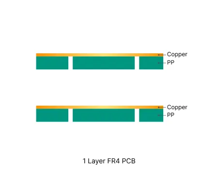
                    1-layer FR4 PCBs begin with copper-clad laminate. Mechanical drilling creates all required holes before electroless plating. Core Steps Pattern imaging followed by copper etching defines circuit traces. Solder mask application and surface finish complete the base process. Surface finish selection balances solderability, cost, and shelf life. Key risk control centers on etch uniformity and precise solder mask registration to maintain yield.

                    Manufacturing Order Profile

                    Order Quantity Order Proportion Estimated Price Level Typical Lead Time
                    Prototype (<=30 pcs) 29% From $1 From 1 Day
                    Small volume (30-200 pcs) 42% From $20 From 1 Day
                    Mass production (>200 pcs) 29% From $40 From 1 Day

                    Manufacturing Challenges & Process Optimization

                    Etching Uniformity

                    Single layer boards frequently require consistent trace widths especially near fine pitch components. Variations in etchant concentration, temperature, and spray pressure across large panels create differential etch rates.

                    Resulting trace width deviation increases resistance in power circuits and risks shorts in dense layouts. This directly reduces both production yield and field reliability.

                    Deploy real-time etchant monitoring systems with frequent chemical analysis.

                    Apply etch factor compensation in design rules and maintain strict spray pressure calibration.

                    Perform automated optical inspection immediately after etching on every panel.

                    Design Considerations

                    Stackup Design

                    Single layer boards require no multilayer planning. Uniform copper distribution across the panel helps control thermal warpage during processing and assembly.

                    Via Strategy

                    Only plated through holes are possible. Minimize hole quantity to control drilling cost. Component leads frequently provide necessary electrical connections.

                    Material Selection

                    Standard FR4 suits most applications. Higher Tg variants improve thermal stability during lead-free soldering. Material selection must match operating environment requirements.

                    Surface Finish

                    HASL offers low cost with good solderability. OSP provides flat surfaces for SMT. ENIG delivers superior oxidation resistance but raises cost for basic single layer designs.

                    Get in Touch