




Typical Specification Range
| Parameter | Typical Range |
|---|---|
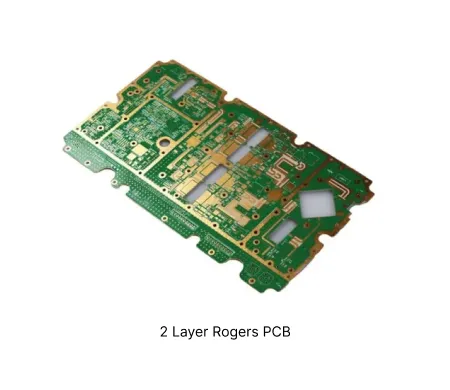
| Layer count | 2 layers |
| Material type | Rogers RO4350B, RO4003C, RT/duroid 5880 |
| Surface finish | ENIG, Immersion Silver, OSP |
| Thickness | 0.101mm to 0.762mm |
| Solder mask | Green, Black, Blue |
| Copper thickness | 0.5oz to 2oz |
| Special features | Controlled impedance, low loss tangent, precise registration |
Manufacturing Process Insights
Lamination
Rogers core is bonded with copper foil under tightly controlled temperature and pressure.
Drilling
Specialized parameters and tools minimize smear on PTFE substrates. Plasma desmear follows to clean hole walls.
Plating
Electroless copper seed layer enables reliable via metallization before pattern plating.
Surface Finish Logic
ENIG is selected to maintain smooth surface for RF performance while ensuring assembly compatibility.
Risk Control
In-process impedance testing and cross-section verification prevent field failures.
Manufacturing Order Profile
| Order Quantity | Order Proportion | Estimated Price Level | Typical Lead Time |
|---|---|---|---|
| Prototype (<=30 pcs) | 65% | From $140 | From 7 days |
| Small volume (30-200 pcs) | 25% | From $150 | From 8 days |
| Mass production (>200 pcs) | 10% | From $300 | From 10 days |
Manufacturing Challenges & Process Optimization
PTFE Drilling Smear
Mechanical drilling of Rogers PTFE materials frequently leaves residue on via barrel walls.
Material softness and high melting point prevent clean cutting and promote heat-induced smearing.
Residue blocks electroless copper adhesion causing plating voids. This reduces yield and creates intermittent via failures under thermal stress.
Utilize peck drilling cycles with specialized bits and reduced feed rates.
Apply plasma desmear process optimized for fluoropolymer substrates.
Validate plating integrity through cross-section analysis and IST testing.
Design Considerations
Core thickness selection determines impedance value. Copper roughness must be factored into calculations. Balanced construction minimizes board bow.
Through vias are standard for 2 layer boards. Backdrilling reduces stub effects at microwave frequencies. Avoid unnecessary blind vias due to added cost.
Match DK and dissipation factor to operating frequency. RO4350B balances performance with processability. Verify material availability against production volume.
ENIG provides flat surface required for RF signals. Avoid HASL due to uneven topography. Gold thickness affects both solderability and long term oxidation resistance.