






Typical Specification Range
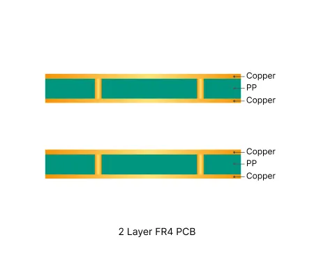
| Parameter | Typical Range |
|---|---|
| Layer count | 2 layers |
| Material type | FR4 TG130 to TG170 |
| Surface finish | HASL, ENIG, OSP |
| Thickness | 0.8mm – 2.0mm |
| Solder mask | Green, black, red, white, yellow, blue, purple, matte black |
| Copper thickness | 1oz – 6oz |
| Special features | Plated through holes, castellated holes |
Manufacturing Process Insights
Material Preparation & Lamination FR4 core is laminated with copper foil under controlled heat and pressure. Symmetrical copper weight is critical to minimize warpage on thin or large panels.
Precision Drilling CNC drilling forms all through-holes. Parameters and tooling are optimized for holes >2.0 mm or high-aspect-ratio boards to control wall roughness, diameter tolerance and registration.
Desmear & Electroless Copper Resin smear is removed and electroless copper deposited to establish conductivity. Uniform coverage at this stage determines long-term via reliability.
Pattern Imaging & Etching Dry film defines the circuit pattern, followed by controlled etching. Precise registration and etch compensation prevent undercut and open circuits on tight features.
Solder Mask Application Liquid photoimageable mask is applied and developed. Via tenting vs open-window decisions are finalized here to avoid ink intrusion and exposed copper.
Surface Finish HASL, ENIG or OSP is selected based on solderability, cost and shelf life. Process control ensures uniform coverage while maintaining dimensional stability.
Routing, V-Scoring & Depanelization Boards are separated by routing, V-scoring or both. Tab width, stamp holes and copper-to-edge clearance are verified to prevent breakage and edge defects.
Electrical Test & Final Inspection 100% electrical testing confirms continuity and isolation. Final inspection against IPC criteria ensures only compliant boards are shipped.
Manufacturing Order Profile
| Order Quantity | Order Proportion | Estimated Price Level | Typical Lead Time |
|---|---|---|---|
| Prototype (<=30 pcs) | 62% | From $1 | From 1 Day |
| Small volume (30-200 pcs) | 26% | From $30 | From 1 Day |
| Mass production (>200 pcs) | 12% | From $50 | From 1 Day |
Manufacturing Challenges & Process Optimization
Via Tenting / Open Via Conflict
Via treatment frequently mismatches between system order notes and Gerber solder mask data.
Designers often specify “open vias” while Gerber shows partial or full tenting (or vice versa).
This leads to inconsistent HASL results, solder bead entrapment, ink intrusion into barrels, exposed copper at via mouths, and long-term reliability risks (oxidation, intermittent connections) that fail IPC-A-600 criteria.
✓ Confirm exact via treatment (full tenting / selective tenting / open) with annotated screenshots before CAM release.
✓ Regenerate solder mask layers to strictly match confirmed intent and apply consistent expansion.
✓ For thick boards (>3 mm) or high-aspect-ratio vias, pre-compensate drill size (e.g. 0.4 mm → 0.6 mm) to improve tenting reliability.
Design Considerations
Always generate solder-mask Gerber layers that exactly match the via treatment stated in the order notes or fabrication notes. For selective tenting, provide a clear list or graphical call-outs of which vias are tented. On boards thicker than 3 mm, evaluate drill compensation early to ensure reliable tenting and plating. Open vias should be reserved only when probe or soldering access is truly required.
Design connection tabs with adequate width for the board thickness and always include stamp holes (mouse bites) when using routing separation. Generate single-board and panelized data from the identical source geometry. Keep critical features, copper and legend completely clear of V-cut or scoring lines. For narrow or long boards, even if single-piece shipment is requested, consider factory panelization with tooling holes and fiducials to maintain registration accuracy.
Maintain ≥0.3–0.5 mm clearance between any pad, trace or copper feature and the final board outline, especially on V-cut panels. Avoid placing holes exactly on the outline. Clearly define process-edge requirements and ensure outline data (GKO / milling layer) is consistent across all files. For Class 3 boards, treat edge condition as a critical reliability item.
Never design PTH pads with zero annular ring. Provide realistic tolerances for holes larger than 2.0 mm after consulting process capability (especially on large panels). Always define solder-mask openings for every PTH hole. Explicitly annotate NPTH vs PTH intent and any selective plugging requirements with reference images or drill lists.