





HDI PCB manufacturing is defined by one fundamental difference from conventional multilayer production: the controlled formation, filling, and stacking of laser-drilled microvias. This guide addresses the complete HDI production process from the microvia perspective, covering every critical stage that determines density, yield, reliability, and cost.
Readers will find a systematic examination of HDI board structures, laser drilling principles and process windows, copper and epoxy microvia filling materials and methods, sequential build-up flow for any-layer interconnect, in-process inspection and reliability testing, real manufacturing case studies, and the dominant cost drivers.
The content is written for process engineers, design engineers, procurement specialists, and technical decision-makers who need to understand not only what HDI is, but how microvia technology shapes every manufacturing decision, and final reliability qualification. By focusing on the microvia as the central process element, the guide provides the practical engineering logic required to specify, manufacture, and qualify HDI boards for high-density applications.
What Is HDI PCB Manufacturing?
An HDI PCB is a printed circuit board that achieves significantly higher wiring density than a conventional multilayer board. It does this by using laser-drilled microvias, sequential build-up layers, and finer traces and spaces. Instead of relying mainly on mechanically drilled through-holes that pass through the entire board, an HDI board connects only the layers that need to be linked. This approach allows more routing channels in a smaller area and supports finer-pitch components such as high-density BGAs.
Conventional boards rely on large mechanically drilled through-holes that consume routing space and create long stubs. HDI manufacturing replaces most of these with small microvias that connect only the needed layers. This reduces pad size, shortens signal paths, and allows more traces to fit between fine-pitch components.
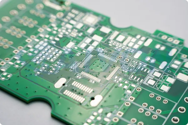
Microvias are the core of HDI production. The ability to form, clean, fill, and stack these tiny laser-drilled holes determines whether higher-density structures can be built reliably. Poor microvia quality leads directly to registration problems, voids, and early failures, which is why every major process step in HDI manufacturing centers on microvia control.
HDI PCB Types and Structures
HDI boards are classified by sequential build-up architecture. Structure determines process sequence, via architecture options, material selection, yield, and ultimately cost and reliability. Misclassification of structure remains a primary source of cost overruns and reliability failures.
|
Construction |
Typical Via Type |
Relative Density |
Relative Cost |
Typical Applications |
|---|---|---|---|---|
|
1+N+1 |
Blind microvias + core through-holes |
Moderate |
Lowest |
Consumer, mid-density modules |
|
2+N+2 |
Stacked or staggered microvias |
High |
Medium |
Smartphones, automotive ADAS |
|
Any-layer |
Fully stacked microvias on every layer |
Highest |
Highest |
AI modules, high-layer-count compute, ultra-thin wearables |

1+N+1 structure
The 1+N+1 structure places a single build-up layer on both sides of a conventional multilayer core. Microvias connect only the outer layers to the adjacent core layers. This configuration supports moderate-density designs with 0.5–0.65 mm pitch BGAs at relatively low cost and is the most common entry-level HDI construction.
2+N+2 structure
The 2+N+2 and higher sequential build-up structures add two or more dielectric and copper layers on each side of the core. Each additional pair requires another lamination, laser-drill, and plating cycle. These structures enable stacked or staggered microvias and support finer-pitch packages down to 0.4 mm.
Any-layer structure
Any-layer or ELIC structures remove the distinction between core and build-up. Every dielectric layer is laser-drilled and filled so that a microvia can connect any pair of adjacent layers. This architecture delivers the highest wiring density and the thinnest constructions, yet it multiplies laser and plating cycles and places the strictest demands on registration accuracy and dielectric thickness uniformity.
Three Microvias in HDI PCBs

Within these structures three via architectures are available. Staggered microvias offset successive vias laterally, reducing registration risk and eliminating the need for complete copper fill. Stacked microvias align vertically to form a continuous copper column, maximizing density and enabling true via-in-pad designs, but they demand void-free fill and precise registration at every interface. Skip vias and combinations of microvias with mechanical through-holes provide additional routing flexibility when selective layer connections are required.
Typical cross-sections show the progression clearly: a 1+N+1 board contains single-depth microvias landing on the outer core layers; a 2+N+2 section reveals either staggered or stacked pairs; an any-layer micrograph displays continuous stacked columns running through the full thickness. Capture-pad size, residual copper at the via bottom, and plating uniformity remain the measurable indicators of process capability for each type.
HDI PCB Material for Sequential Build-Up
HDI boards rely on a combination of core and build-up materials that must work together through multiple lamination and laser-drilling cycles. The core is usually a high-Tg FR-4 or similar rigid laminate chosen for dimensional stability. It provides the mechanical backbone that keeps the board flat while thinner layers are added on both sides.
On top of the core, manufacturers apply specialized build-up dielectrics. Resin-coated copper (RCC) is widely used because its resin formulation supports clean laser ablation and strong adhesion to copper. Laser-drillable prepregs serve the same purpose. These thin dielectrics allow microvias to be formed accurately while keeping the overall board thickness low. Their thickness is tightly controlled, since even small variations affect impedance and the aspect ratio of the vias.

Copper also plays a dual role. Thin electrodeposited copper foils are preferred for fine-line etching on the outer and build-up layers. After laser drilling and desmear, an electroless copper seed layer is deposited, followed by electrolytic plating that builds the circuit traces and fills the microvias. The plating system must deliver good throwing power so that small vias can be filled uniformly without voids.
Material selection influences nearly every subsequent process step. Dielectrics that laser-drill cleanly leave less residue and improve plating adhesion. Stable core materials reduce warpage during sequential lamination. Copper foils and plating chemistries that support fine features and void-free filling determine whether stacked microvias can be produced reliably. Choosing materials that match the laser, desmear, and plating processes is therefore essential for consistent yield and long-term reliability in HDI manufacturing.
Microvia Technology in HDI PCB Manufacturing
Microvia Formation and Laser Drilling
Microvias are the single biggest reason HDI boards can achieve much higher density than conventional multilayer boards. Instead of drilling all the way through the board with a mechanical drill, manufacturers use a laser to create very small holes that only connect the specific layers needed. The quality of these laser-drilled holes largely decides how well the vias can be plated later, how reliable stacked structures will be, and how many defects appear in production.
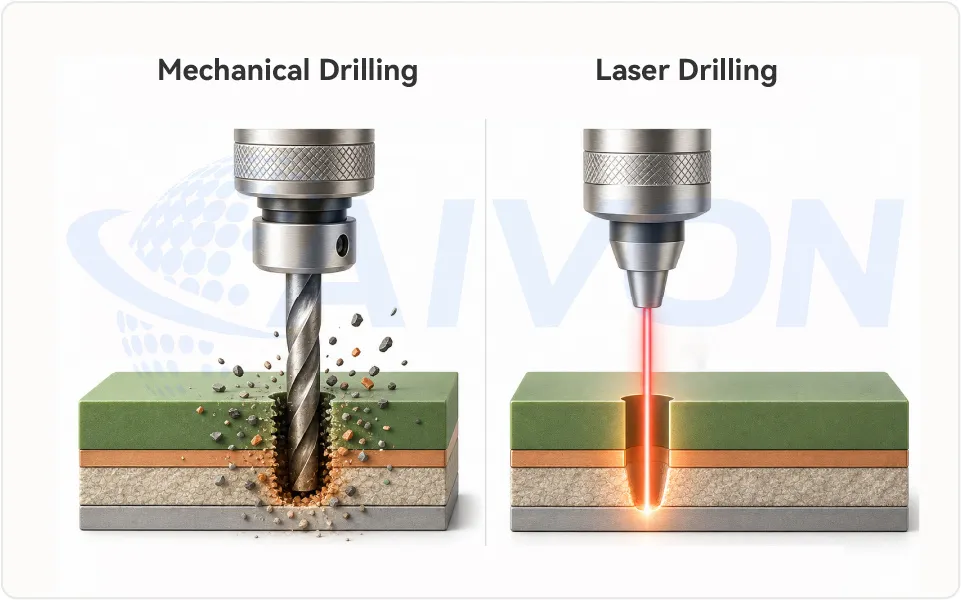
The laser removes the dielectric material in one of two ways. Some lasers mainly heat the material until it vaporizes, which is called photothermal ablation. Others break the chemical bonds in the resin more directly while also generating some heat, which is called photochemical ablation.
CO₂ lasers work primarily by heating. They are fast and economical, which makes them the common choice for vias larger than about 75 µm. UV lasers combine bond-breaking with heating. They create cleaner sidewalls and can produce much smaller vias, often down to 25 to 50 µm.

Which laser works best depends on the dielectric material itself. Different resins absorb laser energy differently. The material’s glass-transition temperature and the amount of filler it contains also influence how cleanly the laser can cut and how much residue is left behind.
Once the laser type is chosen, four practical settings control the final hole shape: the energy of each pulse, how many pulses are fired per second, the size of the laser spot, and the exact focus position. These settings determine the entrance diameter at the top of the via, how much the sidewalls taper, and how much copper remains at the bottom. Too much energy can make the hole too wide or damage the landing pad. Too little energy leaves resin residue that later causes plating problems.

After the laser finishes drilling, a cleaning step called desmear is essential. Chemical or plasma treatment removes any remaining resin smear and prepares the surface so copper can adhere properly. Incomplete desmear is still one of the most common reasons for poor adhesion and voids in the finished microvia.
Methods of Microvia Filling

The microvia filling process employs distinct methods tailored to material type and production scale. Copper filled microvias rely on electrolytic plating, starting with electroless copper seed layer deposition after laser drilling and desmear. Pulse reverse electroplating then fills the via from bottom to top, minimizing voids through controlled current density and reversal. This super-filling technique creates a slight dome or flat top, which lamination flattens. Epoxy filled microvias use screen printing or vacuum-assisted dispensing to inject paste into vias, followed by thermal curing.
For copper filling, the process sequence includes panel electroplating for initial barrel plating before targeted via filling. Reverse pulse plating parameters adjust additive concentrations to promote uniform growth. Epoxy methods accommodate higher aspect ratios since paste flows under pressure, but require stencil design for precision. Hybrid approaches combine conductive paste with plating for through-hole filling in complex boards. Factories optimize these methods per IPC guidelines to achieve consistent results across panels.
Conductive pastes for epoxy filled microvias incorporate metal flakes suspended in resin, screened through fine meshes matching via pitch. Curing schedules align with board bake-out to prevent outgassing. Copper methods demand cleanroom controls to avoid contamination during plating baths. Both approaches cap filled vias with photoresist or dielectric for protection.
HDI PCB Manufacturing Process and Key Challenges
HDI boards are built using a sequential process rather than the single lamination cycle used for conventional multilayer boards. The manufacturer starts with a core, then adds dielectric and copper layers one step at a time, drilling and plating microvias after each addition. This sequence is repeated until the required number of build-up layers is reached.
A typical cycle includes the following steps: dielectric material, such asprepreg or resin-coated copper, is laminated onto the existing structure, the laser drills the microvias to the target pads, desmear cleans the holes, electroless and electrolytic copper are applied to form the interconnect, and the circuit pattern is imaged and etched. After inspection, the next dielectric layer is added and the cycle begins again.
For simple 1+N+1 designs the sequence happens only once on each side. For 2+N+2 or higher constructions the same sequence is repeated multiple times.
Three practical challenges dominate the HDI manufacturing process and largely determine yield and final quality.
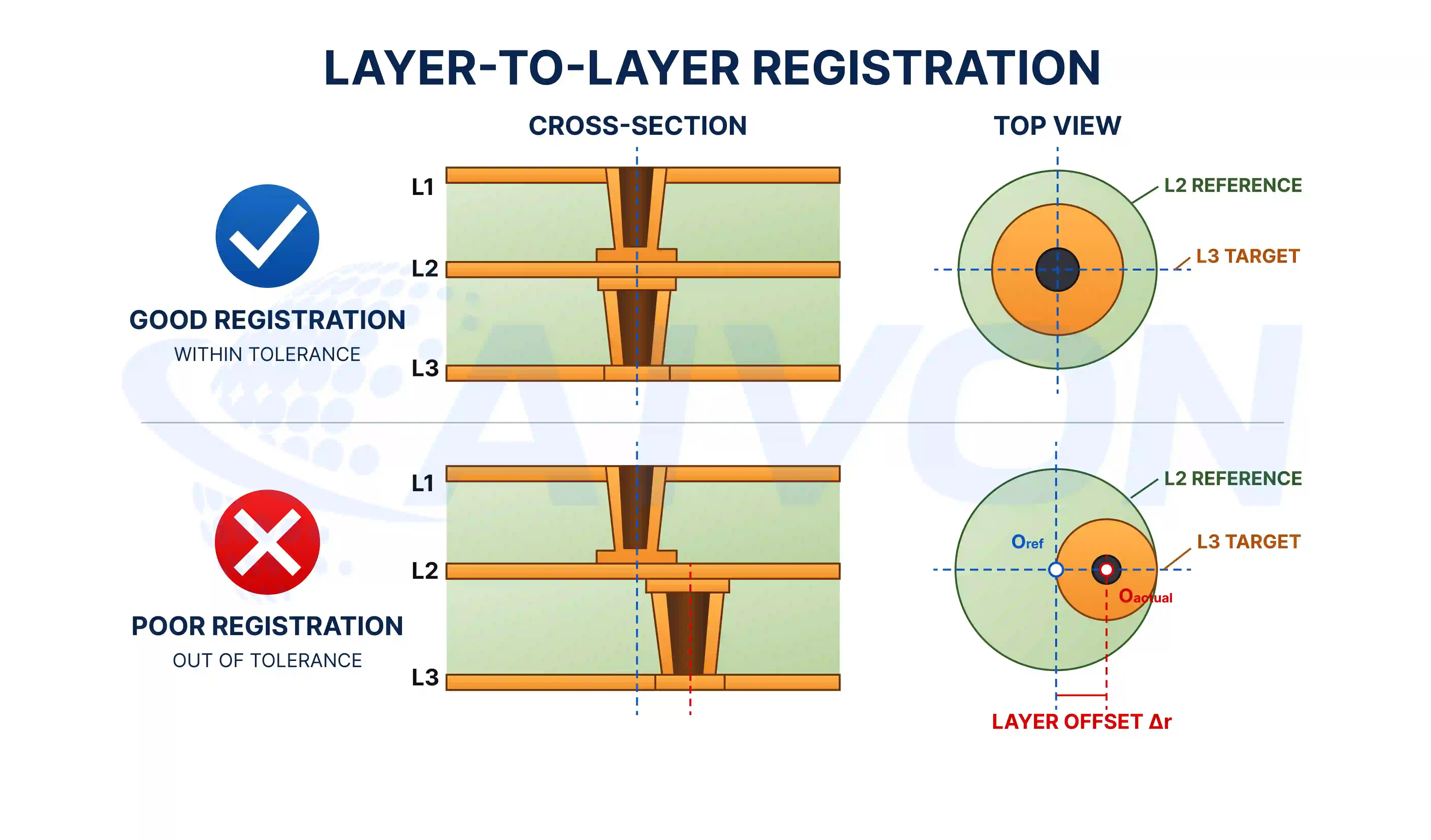
The first is layer-to-layer registration. Each new set of microvias must land accurately on the pads of the previous layer. Even small misalignment accumulates as more layers are added, so optical or X-ray alignment systems and careful compensation are required to keep the error within acceptable limits.

The second challenge is dielectric thickness and surface flatness. The thickness of each new dielectric layer must stay consistent across the panel. Variation affects impedance control and also changes the laser focus for the next drilling step. Uneven surfaces after plating or planarization make it harder to achieve reliable registration on the following layer.

The third challenge is residual stress and warpage. Every lamination and plating step introduces stress into the board. As more sequential layers are added, the stress builds up and can cause the panel to warp. Symmetric copper distribution, controlled cooling after lamination, and occasional intermediate stress-relief steps are used to keep warpage within the limits needed for fine-pitch assembly.
These three issues become more demanding as the number of sequential cycles increases. Process capability in registration accuracy, thickness control, and warpage management therefore sets the practical limit on how complex an HDI structure can be manufactured reliably.
HDI PCB Manufacturing Quality Control and Reliability Testing
HDI boards contain many internal features that cannot be checked by simple visual inspection. Because microvias, stacked connections, and thin dielectric layers are hidden inside the board, manufacturers must use a combination of in-process checks, non-destructive testing, and formal reliability testing to ensure consistent quality.

During production, automated optical inspection (AOI) is used on outer layers to catch pattern defects, opens, and shorts. For internal features such as buried or stacked microvias, X-ray inspection is essential. X-ray can reveal voids, incomplete fills, and misregistration that would otherwise go unnoticed until the board fails later.

CEZON also take microsection samples at key process steps. These cross-sections allow engineers to measure plating thickness, check for residual resin, and confirm that the via walls and interfaces are properly formed.
After the boards are completed, reliability testing is performed to verify that the structure can survive the stresses of assembly and field use. Common tests include thermal cycling, interconnect stress testing (IST), and conductive anodic filament (CAF) testing.
|
Test |
Purpose |
|---|---|
|
Thermal Cycling |
Checks for cracks or opens caused by repeated temperature changes. |
|
IST |
Monitors resistance during rapid heating and cooling to detect developing failures. |
|
CAF Testing |
Evaluates the risk of conductive path formation under humidity and electrical bias. |
Several HDI microvia defects and failure modes appear more often in HDI than in conventional boards. Corner cracks can form at the bottom of a microvia if the laser hole is poorly shaped or residual stress is high. Interface separation can occur between stacked vias when the copper fill is incomplete. CAF growth may develop along moisture paths or contaminated interfaces. Warpage caused by uneven stress during sequential lamination can also affect assembly yield.
Manufacturers reduce these risks through process control rather than relying only on final testing. They keep microvia aspect ratios moderate, ensure thorough desmear after laser drilling, maintain tight control of plating chemistry, bake boards to remove moisture, and use symmetric copper distribution to limit warpage. Each production lot is typically qualified against the specific thermal and humidity conditions of the end application, following the relevant IPC performance class requirements. This combination of in-process inspection, targeted reliability testing, and disciplined process control is what allows HDI boards to meet the demands of high-density applications.
CEZON’s HDI PCB Fabrication and Manufacturing Capabilities
CEZON maintains tight process control over the critical parameters that directly affect HDI interconnect reliability, dimensional accuracy, and production yield.
|
Key HDI Control |
CEZON Process Control |
Why It Matters |
|---|---|---|
|
Microvia Filling |
Blind-via dimple controlled to ≤25 μm |
Ensures reliable microvia structures and supports high-density interconnections |
|
Hole Accuracy |
PTH: ±0.076 mm; NPTH: ±0.05 mm |
Maintains accurate interlayer connections and component alignment |
|
Fine-Line Control |
Trace width/spacing tolerance controlled to ±20% |
Supports the tight geometries required for high-density HDI layouts |
|
Board Flatness |
Board warpage controlled to ≤0.75% |
Helps maintain dimensional stability during assembly |
|
Plating & Copper Distribution |
Auxiliary copper patterns can be added to balance plating |
Reduces plating imbalance and helps control board warpage |
|
Quality & Traceability |
Electrical testing and production traceability marking |
Provides additional verification and process traceability |
These controls demonstrate that CEZON’s HDI manufacturing is not limited to standard PCB production. We actively evaluate microvia geometry, via filling, drilling tolerances, copper distribution, and board deformation during engineering review and production to ensure that the design can be manufactured reliably.
Rather than simply following the supplied Gerber files, CEZON’s engineering team reviews critical HDI structures and identifies potential manufacturing risks before production. When a design uses non-standard laser-drilled blind vias or buried vias that may affect filling and reliability, we evaluate the structure and recommend manufacturable dimensions accordingly.
Real HDI PCB Manufacturing Case: Optimizing Blind and Buried Via Dimensions
For one HDI project, the customer’s Gerber files specified 0.2 mm blind vias between IN1–1/2 and IN4-Back–6/5. Because CEZON manufactures HDI blind vias using laser drilling, this diameter was outside the preferred range for the laser-drilled structure.
During engineering review, CEZON identified the issue and recommended reducing the blind-via diameter from 0.2 mm to 0.1 mm to better suit the laser drilling process.
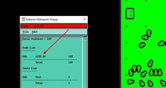
The same design contained 0.6 mm buried vias. Since a large buried via diameter can make via filling more difficult, CEZON recommended reducing the diameter to 0.3 mm to improve manufacturability and filling performance.
|
Design Feature |
Customer Gerber |
CEZON Recommendation |
Engineering Consideration |
|---|---|---|---|
|
Blind Via |
0.2 mm |
0.1 mm |
Optimized for laser drilling |
|
Buried Via |
0.6 mm |
0.3 mm |
Improves via-filling manufacturability |
This case demonstrates CEZON’s DFM-driven HDI engineering capability: we don’t simply manufacture according to the submitted files. Our engineers evaluate whether critical HDI structures are compatible with the actual manufacturing process and proactively recommend design adjustments to improve manufacturability, yield, and interconnect reliability.
Conclusion
HDI manufacturing is built around the microvia. The choice of board structure, the precision of laser drilling, the quality of via filling, and the control of sequential build-up all depend on how well these small interconnects are formed and maintained. When registration, dielectric thickness, and warpage are kept under control, denser and more complex designs become manufacturable at practical yields.
In-process inspection, targeted reliability testing, and clearly defined process limits turn these technical requirements into consistent results. Boards that pass these controls deliver the higher interconnect density, shorter signal paths, and long-term reliability that modern electronics demand.
Understanding the complete chain, from microvia formation through final process discipline, allows engineers and procurement teams to specify and produce HDI boards that perform as intended.
FAQs
Q1: What Is HDI PCB Technology?
A1: HDI PCB technology is an advanced PCB manufacturing approach that uses fine-line traces, microvias, sequential build-up structures, and high-density routing to fit more interconnections into smaller boards. It enables compact designs, shorter signal paths, improved electrical performance, and higher component density. HDI technology is widely used in smartphones, automotive electronics, medical devices, telecommunications, and other high-performance electronic products.
Q2: What Latest Techniques Enable High-Precision Impedance Control in HDI PCBs?
A2: Latest HDI techniques for high-precision impedance control include advanced stackup design, tightly controlled dielectric thickness, fine-line routing, low-loss materials, optimized copper thickness, and continuous reference planes. 3D electromagnetic simulation and automated impedance analysis can further verify high-speed structures before fabrication. These methods help control trace impedance, minimize signal reflections and crosstalk, and improve signal integrity in high-density PCB designs.
Q3: What is the practical difference between staggered and stacked microvias in terms of reliability?
A3: Staggered microvias eliminate the copper-to-copper interface between successive microvias, removing a common crack-initiation site. Stacked microvias concentrate stress at each filled junction, making void-free plating and tight process control essential. For applications requiring more than two stacked levels, staggered or hybrid architectures generally provide higher field reliability with lower process risk.
Q4: When does any-layer HDI become more cost-effective than sequential 2+N+2?
A4: Any-layer HDI generally costs more than 2+N+2 until the required interconnect density makes the higher process cost worthwhile. The crossover can occur when package pitches fall below approximately 0.3 mm or when total board thickness must remain below about 0.6 mm and conventional sequential build-up cannot provide sufficient routing density.
Q5: What laser parameters most strongly affect via fill quality?
A5: Entrance diameter, taper angle, and residual copper thickness at the via bottom strongly affect subsequent plating quality. Laser energy density and pulse count must be optimized to produce clean via bottoms and residue-free sidewalls. Because different dielectric materials respond differently to laser energy, material-specific process windows are essential.
Q6: What are the dominant cost drivers in HDI production?
A6: The major HDI cost drivers include sequential lamination cycles, copper-fill and planarization processes, laser drilling time, and yield losses caused by registration or via-fill defects. Higher-performance materials can add cost, but the number of additional process steps usually has a greater impact on the overall HDI premium.
Q7: What IPC/industry standards govern HDI microvia acceptance?
A7: IPC-6012 and IPC-6016 define relevant performance requirements and microvia criteria, while IPC-2226 provides HDI design guidance and classification. Automotive and aerospace applications may also require additional thermal cycling, interconnect stress testing (IST), and customer-specific reliability requirements beyond the baseline IPC standards.
Q8: How do different dielectrics change laser drilling and plating windows?
A8: Different dielectric materials require different laser and desmear process windows. High-filler FR-4 may require higher laser energy and more aggressive desmear, while polyimide and PTFE-based materials can ablate more readily but may leave residues that require thorough removal. Low-loss materials may also benefit from UV laser processing for cleaner sidewalls and require tighter control of plating chemistry to maintain adhesion.
Q9: What are the main differences between copper-filled microvias and epoxy-filled microvias?
A9: Copper-filled microvias use electroplating to create a conductive metallic fill, providing excellent electrical conductivity and heat transfer and making them well suited for stacked vias and high-current applications. Epoxy-filled microvias use a resin-based fill and are generally lower cost, making them suitable for applications where insulation or simpler processing is sufficient. Copper fills typically offer better thermal-cycle reliability, while epoxy fills can be more susceptible to stress and delamination due to differences in thermal expansion.
Q10: Which companies can produce HDI boards with laser drilling capabilities?
Companies with HDI manufacturing capabilities typically use CO₂ or UV laser drilling systems to produce microvias for high-density multilayer boards. At Cezon, our HDI production processes support laser-drilled microvias, sequential buildup, blind vias, and fine-line routing. Engineers can select laser parameters according to dielectric thickness, via diameter, and material characteristics to achieve consistent drilling quality and reliable interlayer connections.


