

FR-4 PCB Design Fundamentals: A Beginner’s Step-by-Step Guide

Understanding FR-4 Material in PCB Design

If you are new to printed circuit board (PCB) design and planning to create your initial board using FR-4 material, this guide is an ideal starting point. It will navigate you through the core aspects of FR-4 PCB design for beginners, encompassing everything from comprehending the material’s properties to designing both single-layer and double-layer boards with widely used software tools. This step-by-step tutorial offers actionable insights to help you commence your design journey.

This comprehensive article will deeply explore the process of designing with PCB FR4 material, which is the most common material utilized for printed circuit boards globally. You will grasp the foundational principles of PCB design with FR-4, discover various software options, and follow detailed instructions for crafting both single-layer and double-layer designs.
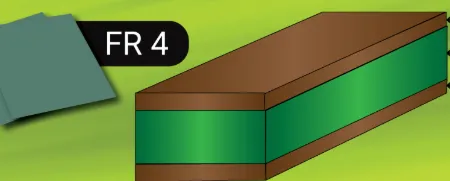
FR-4 Material in PCB Design

What Exactly Is FR-4?

FR-4 is a specific type of fiberglass-reinforced epoxy laminate that functions as the foundational material for the majority of printed circuit boards. The “FR” abbreviation denotes “Flame Retardant,” indicating its inherent fire-resistant properties, which makes it a secure choice for diverse electronic applications. Its widespread adoption stems from its balanced combination of affordability, robust durability, and effective electrical insulation characteristics, rendering it suitable for both novice designers and seasoned professionals.

FR-4 possesses a dielectric constant of approximately 4.5, which is well-suited for a broad spectrum of low to medium-frequency applications. It also provides commendable mechanical strength, ensuring that your PCB can withstand physical stresses during both assembly and operational use. For hobbyists and engineers working on either single-layer or double-layer FR-4 PCB designs, this material is frequently the preferred option due to its lower circuit board cost and versatile applications.

Related Reading: Exploring the World of Multilayer FR-4 PCBs: Design, Manufacturing, and Applications

Initial Steps for FR-4 PCB Design: Tools and Preparation

Before delving into the actual design phase, it is essential to assemble the appropriate tools and prepare your work environment. The primary step involves selecting the right FR-4 PCB design software that aligns with your current skill level and project specific requirements. Below are three highly recommended options suitable for beginners:

Popular Design Software for Beginners

● Eagle: This tool is known for its user-friendly interface, extensive community support, and vast component libraries, making it an excellent starting point for learning FR-4 PCB design.

● KiCad: As a free, open-source software suite, KiCad is an ideal choice for hobbyists and students, offering a comprehensive set of features for schematic capture and PCB layout.

● Altium Designer: Representing a professional-grade solution, Altium Designer is geared towards more intricate designs, providing advanced functionalities for complex PCB development.

Beyond software, you will also need a fundamental understanding of your project’s requirements. This includes defining the circuit’s intended function, identifying all necessary components, and determining whether a single-layer or double-layer board will best suit your needs. Single-layer boards are simpler to design and typically less expensive, whereas double-layer boards accommodate more complex circuits and offer superior signal routing capabilities.

Step-by-Step Tutorial for FR-4 PCB Design

With your tools ready, let’s proceed with the process of designing a PCB using FR-4 material. This guide covers both single-layer and double-layer FR-4 PCB designs, with specific distinctions highlighted where applicable.

Step 1: Define Your Circuit Requirements

Begin by meticulously outlining the functional requirements of your circuit. Compile a comprehensive list of all components, such as resistors, capacitors, and microcontrollers, along with their precise specifications. For example, if designing a straightforward LED circuit, note the required voltage (e.g., 5V) and current draw (e.g., 20mA per LED). This foundational step ensures that your final board design will precisely meet your project’s electrical and physical demands.

Step 2: Create a Schematic Diagram

Using your chosen PCB design software, construct a schematic diagram that visually represents your circuit. This diagram serves as an electrical blueprint, illustrating how all components are interconnected. In software environments like KiCad or Eagle, you can easily drag and drop components from their respective libraries and establish connections using virtual wires. Verifying the accuracy of all connections at this stage is crucial to prevent significant issues later in the PCB design process. For beginners using KiCad, start by opening the schematic editor, adding components, and clearly labeling nets for enhanced clarity. In Eagle, the procedure is similar, with an emphasis on selecting appropriate library parts. Altium Designer provides more sophisticated features, including real-time error checking, which can proactively identify mistakes.

Step 3: Design the PCB Layout

Once your schematic is finalized, transition to the PCB layout editor within your software. This phase involves arranging components physically on the FR-4 board and routing the copper traces that electrically connect them. For a single-layer FR-4 PCB design, all traces must be confined to one side of the board. In contrast, for a double-layer FR-4 PCB design, you have the flexibility to utilize both sides, which permits shorter traces and inherently reduces electromagnetic interference.

Keep the following tips in mind during the layout phase:

● Place components logically, grouping related parts together to minimize trace lengths.

● On single-layer boards, endeavor to avoid crossing traces; use jumpers if absolutely necessary.

● For double-layer designs, employ vias (small plated holes) to establish connections between layers.

● Maintain an appropriate trace width that can safely carry the required current. For example, a trace conducting 1A might need a width of 0.5mm on 1oz copper FR-4 material.

Step 4: Set Design Rules Specific to FR-4 Material

FR-4’s specific material properties directly influence the design rules you must adhere to, particularly concerning impedance and thermal management. Most PCB design software tools allow you to configure constraints such as minimum trace width (e.g., 0.2mm for standard designs) and clearance (e.g., 0.2mm between adjacent traces) to ensure manufacturability. Given FR-4’s dielectric constant of approximately 4.5, which affects signal speed, it is advisable to keep traces short when working with high-frequency designs (above 100MHz). In Altium, these parameters are configured within the design rule editor. Eagle and KiCad offer similar functionalities, typically found in their settings or constraints menus, making them accessible.

Step 5: Route Traces and Optimize Layout

Routing involves drawing the copper traces that establish the electrical connections between components. For a single-layer board, this can be quite challenging due to inherent space limitations, thus requiring meticulous planning. Double-layer boards offer considerably more flexibility, as you can route power and ground planes on separate layers to effectively reduce noise and improve signal integrity.

Pay close attention to signal integrity during routing. For instance, ensure that high-speed signals (above 50MHz) are kept sufficiently isolated from power lines to prevent undesirable interference. Furthermore, utilizing a solid ground plane on one layer of a double-layer board can significantly enhance stability and reduce electromagnetic interference (EMI).

Related Reading: The Ultimate Guide to Connecting Components with Inner Layer Traces

Step 6: Verify and Export Your Design

Before submitting your design for manufacturing, it is imperative to conduct a comprehensive Design Rule Check (DRC) using your software. This check identifies potential errors such as unconnected pins or overlapping traces. Most tools like KiCad, Eagle, and Altium have integrated DRC features that highlight issues visually or through error messages. Once the design is thoroughly verified and error-free, export your design files, typically in Gerber format, which is the industry standard for PCB manufacturing. Ensure that your export settings include all necessary layers for copper, solder mask, and silkscreen.

Single-Layer vs. Double-Layer FR-4 PCB Design: Key Distinctions

The decision between a single-layer FR-4 PCB design and a double-layer FR-4 PCB design largely depends on the complexity of your project. Here’s a concise comparison:

● Single-Layer: Best suited for simple circuits with fewer components. These boards are typically cheaper to manufacture and easier to design, though they offer limited routing options. They are ideal for basic projects such as LED drivers or simple power distribution boards.

● Double-Layer: Recommended for more complex circuits featuring higher component densities. Double-layer boards provide enhanced signal routing capabilities and allow for the implementation of dedicated ground planes, which effectively reduces noise. They are perfect for microcontroller-based designs or projects with multiple integrated circuits.

For beginners, it is often advisable to start with a single-layer board to firmly grasp the fundamentals of basic FR-4 PCB design before progressing to more intricate double-layer designs.
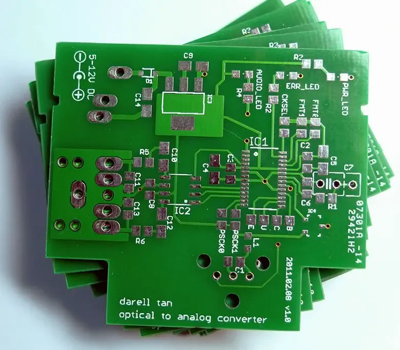
Single-Layer vs. Double-Layer FR-4 PCB Design: Key Distinctions

Selecting the Appropriate FR-4 PCB Design Software

Your choice of FR-4 PCB design software can profoundly influence your learning trajectory and the ultimate quality of your designs. Here’s a detailed breakdown of the three tools previously mentioned, specifically tailored for beginners:

Software Options for FR-4 PCB Design

● Eagle for FR-4 PCB Design: Eagle is well-regarded for its intuitive user interface and extensive component libraries, making it an excellent starting point. It fully supports both single and double-layer designs with user-friendly schematic and layout editors. Its free version is typically sufficient for smaller projects that require up to two signal layers.

● KiCad for FR-4 PCB Design: KiCad is a powerful, free, and open-source tool that rivals commercial software. It offers a complete suite for schematic capture, PCB layout, and even sophisticated 3D visualization of your FR-4 board. Its open-source nature ensures continuous updates and strong community support, making it an excellent choice for a wide range of projects.

● Altium Designer for FR-4 PCB Design: Altium Designer stands as a premium option, primarily targeting professionals and advanced hobbyists. It excels in managing complex double-layer designs, offering advanced features such as interactive routing and precise impedance control for high-speed signals on FR-4 material. While it does present a steeper learning curve, its capabilities for professional-grade design are unparalleled.
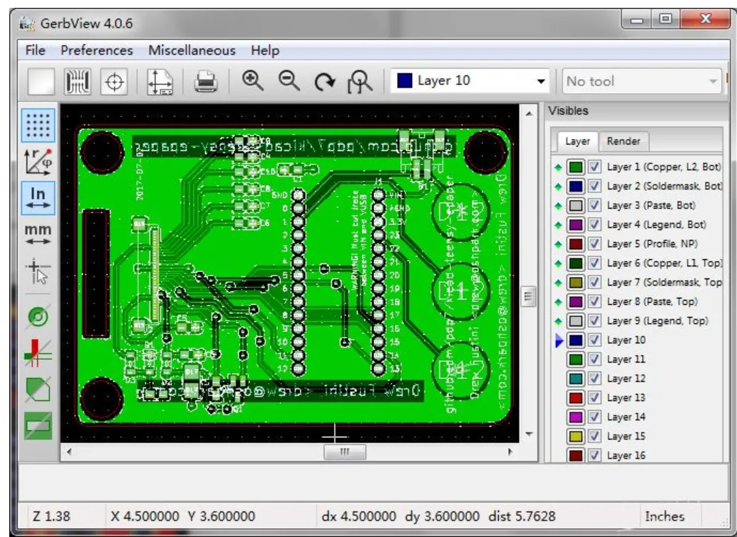
Software Options for FR-4 PCB Design

Practical Tips for Successful FR-4 PCB Design

To conclude, here are some practical tips to ensure your FR-4 PCB design journey is smooth and productive:

● Begin with Simplicity: Always start with small, uncomplicated projects to progressively build confidence in basic FR-4 PCB design principles.

● Verify Component Footprints: Consistently double-check component footprints against their respective datasheets to prevent sizing errors during layout.

● Utilize Ground Planes: For double-layer designs, always incorporate a solid ground plane to effectively minimize noise and enhance signal integrity.

● Shorten Trace Lengths for High Frequencies: Keep trace lengths as short as possible for high-frequency signals to avoid delays, taking into account FR-4’s dielectric constant of 4.5.

● Simulate When Possible: If your chosen software, like Altium, offers built-in simulation tools, utilize them to predict and optimize the performance of your design before fabrication.

Conclusion: Embark on Your FR-4 PCB Design Journey Today

Designing a PCB using FR-4 material is an exciting and entirely achievable endeavor, even for those new to the field. By following this detailed step-by-step tutorial, you have acquired fundamental knowledge concerning both single-layer and double-layer FR-4 PCB design, along with practical guidance on utilizing popular FR-4 PCB design software such as Eagle, KiCad, and Altium. From creating precise schematics to routing efficient traces and exporting manufacturing files, you now possess the essential foundation to transform your electronic concepts into tangible reality.

Whether you are a hobbyist exploring new interests or an aspiring engineer building your portfolio, FR-4 provides a reliable and cost-effective base for a vast array of projects. Select a software tool that suits your needs, commence with a simple design, and gradually tackle more complex boards as your experience grows. With diligent practice, you will master basic FR-4 PCB design and beyond, enabling you to create innovative circuits that power groundbreaking solutions.

Get in Touch


    FR4 PCB Manufacturing: Materials, Process, and Fabrication Guide

    FR4 is not a single laminate. It is a family of glass-reinforced epoxy materials used to manufacture most rigid PCBs. During production, FR4 CCL and prepreg are processed through inner-layer imaging, lamination, drilling, plating, solder mask, surface finishing, and electrical testing. The important point is that FR4 alone does not define Tg, Td, CTE, dielectric properties, or thermal reliability.

    This guide explains both how FR4 laminate is manufactured and how finished FR4 PCBs are fabricated, with practical guidance on material selection, reliability, and manufacturing specifications.

    What FR4 Materials Actually Are?

    FR-4 is a NEMA grade name: Flame Retardant, class 4. The usual flammability target on finished boards is UL 94 V-0. That rating says the coupon extinguishes under a defined flame test. It says nothing about whether the resin will survive two 260 °C reflow peaks without delaminating.

    Construction is consistent across the family: woven E-glass fabric, a brominated or halogen-free epoxy resin system, and electrodeposited copper foil. The product that arrives at a PCB shop is not one sheet. Core is fully cured copper-clad laminate used for inner layers and simple 1 to 2 layer boards. Prepreg is partially cured resin on glass; resin flow and gel time determine fill, thickness, and void risk during multilayer press.

    One label covers many products because the chemistry and construction knobs are independent:

    Design Factor

    Typical Options

    Key Impact

    Resin Functionality

    Difunctional, tetrafunctional, multifunctional epoxies

    Determines crosslink density, Tg, and chemical resistance.

    Filler System

    Inorganic fillers

    Reduces Z-CTE and increases Td, but can increase drill wear and narrow the desmear process window.

    Glass Style

    106, 1080, 2116, 7628

    Influences resin content, finished dielectric thickness, Dk, and the glass-weave effect on impedance.

    Copper Treatment

    STD, RTF, VLP, HVLP foils

    Affects peel strength, etch factor, and insertion loss.

    FR4 Materials: CCL, Prepreg, and Glass Styles

    CCL (copper-clad laminate) is fully cured core. Inner-layer cores are imaged, etched, and oxide-treated before layup. Thin cores and 1–2 layer boards use CCL as the finished dielectric. Thickness tolerance on core is a first-order impedance input; a 0.1 mm core with ±10% thickness scatter already consumes a large fraction of a 10% impedance budget.

    Prepreg is B-stage resin on glass. During press it melts, flows into etched copper topography, and gels. Resin content, volatile content, and gel time are the three incoming parameters that decide whether the stack fills without starvation or squeeze-out. High-resin styles, such as 106, 1080, fill fine features and drop Dk. Glass-rich styles like 7628 add stiffness and raise Dk. Mixing styles without a stackup calculation is how “1.6 mm FR4” boards from two CMs land at different impedances.

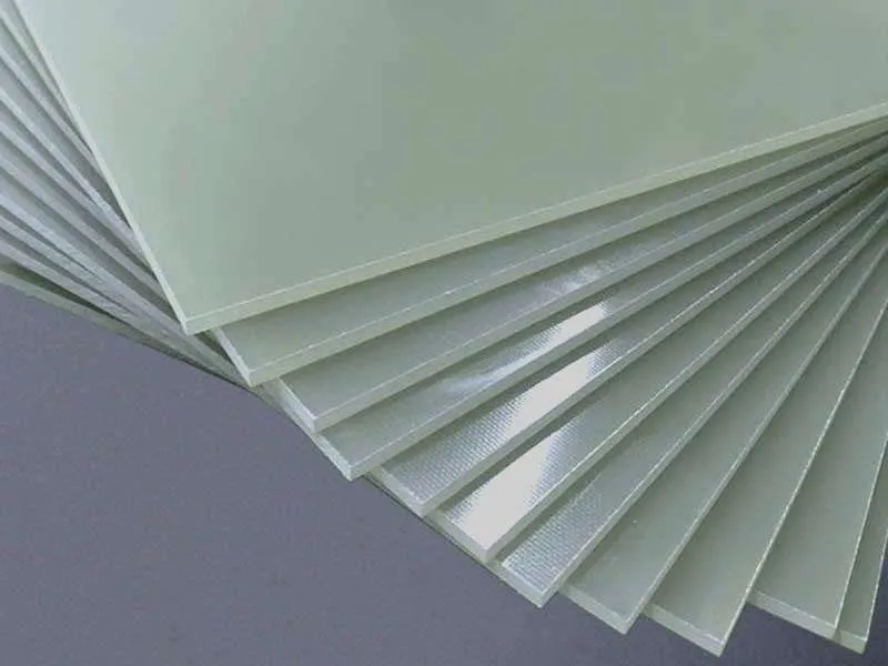
    Unclad FR4 sheet is the same resin family without foil. Procurement follows IPC-4101/21 more often than /24. It is not a PCB core substitute. Using unclad sheet as a last-minute inner dielectric is a process control failure, not a cost save.

    Unclad FR4 sheet

    Finished dielectric thickness is not the nominal prepreg thickness on the datasheet. After press, resin has flowed into the copper pattern. High copper remaining on inner layers reduces compressed dielectric thickness and raises local Dk. Designers who ignore residual copper when calculating stackup will see impedance coupons fail even when the laminate lot is in spec.

    FR4 Grades and Material Properties

    Shop-floor grades are thermal bins, not marketing names:

    FR-4 Type

    Typical Tg

    Typical Examples

    Main Characteristics

    Standard Tg FR-4

    ~130–140 °C

    Shengyi S1141, Nanya NP-140

    General-purpose FR-4 for standard PCB applications.

    Mid-Tg FR-4

    ~150–160 °C

    Nanya NP-155F, Shengyi S1000H

    Higher thermal stability than standard Tg FR-4; suitable for more demanding applications.

    High-Tg FR-4

    ~170–180 °C

    Shengyi S1000-2 / S1000-2M, ITEQ IT-180A, Isola 370HR

    Provides higher thermal resistance and improved reliability for high-temperature processing and applications.

    Halogen-Free FR-4

    Typically mid- to high-Tg

    Br <900 ppm; Cl <900 ppm; Br + Cl <1500 ppm per IEC 61249-2-21

    Uses halogen-free chemistry to meet environmental and material requirements; Tg varies by material system.

    Enhanced-Electrical/Low-Loss FR-4

    Material-dependent

    Glass-epoxy systems with improved electrical performance

    Reduces dielectric loss compared with commodity FR-4 when Df begins to limit high-speed channel length; not equivalent to Rogers high-frequency laminates.

    IPC Standards for FR-4

    FR-4 work is specified against a small set of IPC documents. They do not pick the brand for you. They set the floor the laminate and the finished board have to meet.

    IPC-4101 covers the base material. Slash sheets such as /24, /42, and /99 define what FR4 must deliver for Tg, Td, construction, and halogen status. Put the slash sheet on the drawing if you do not want a generic core.

    IPC-6012 covers the finished rigid board: copper in the hole, plating class, bow and twist, and acceptance for Class 2 or Class 3. Material grade and board class are separate calls.

    IPC-TM-650 is the test methods book behind both. Tg, Td, T-288, peel, moisture, and many reliability screens are run to these procedures. A CoC number without a method is hard to compare.

    FR4 Material Parameters That Affect PCB Manufacturing

    Values below are typical production ranges, not guaranteed limits.

    Parameter

    Standard Tg (TG130)

    Mid-Tg (TG150)

    High-Tg (TG170)

    Why fabrication cares

    Typical Tg

    130–140 °C

    150–170 °C

    170 °C+

    Softening point during reflow and press

    Td

    ~300–310 °C

    ~320–330 °C

    ~340–350 °C

    Irreversible resin breakdown

    Moisture absorption

    0.12–0.18%

    0.10–0.15%

    0.08–0.12%

    Bake, CAF, popcorning

    Dk

    4.2–4.6

    4.2–4.6

    4.1–4.5

    Impedance and stackup

    Df

    0.015–0.025

    0.015–0.025

    0.010–0.020

    Loss at higher bit rates

    Typical layer range

    1–6

    4–12

    8–20+

    Sequential lamination survival

    Relative laminate cost

    1.0×

    1.10–1.20×

    1.20–1.40×

    BOM vs scrap risk

    Example products

    Shengyi S1141, Nanya NP-140

    NP-155F, S1000H

    S1000-2 / S1000-2M, ITEQ IT-180A, Isola 370HR

    Named spec on fab drawing

    Secondary parameters that still belong on a serious RFQ:

    ● Peel strength after thermal stress (IPC-TM-650 2.4.8)

    ● CTI for high-voltage tracking (IEC 60112)

    ● Thermal conductivity, typically about 0.3 W/m·K on unfilled FR4. Filled high-Tg systems can read higher. FR4 is not a heat spreader.

    ● Flexural modulus and dimensional stability after press

    ● CAF resistance rating and test coupon geometry

    How FR4 Laminate and Prepreg Are Manufactured

    Two factories sit in the supply chain. The laminator makes CCL and prepreg. The PCB fabricator turns those sheets into a circuit. Defects that look like fab problems often started as resin content scatter, undercure, or foil treatment variation at the laminator.

    Laminate process step by step:

    1.  Resin formulation. Epoxy, hardener, flame retardant, fillers, solvents, and flow modifiers are mixed to a target viscosity and solids content. Phenolic-cured systems generally deliver higher Td and better lead-free endurance than older dicy systems at the same Tg bin.

    2.  Glass cloth treating / impregnation. Woven E-glass is dipped or coated so resin wets every filament. Incomplete wet-out becomes a CAF path later.

    3.  B-stage drying. Solvent is driven off under controlled heat. The output is prepreg with specified resin content, volatile, and gel time.

    4.  Book build. Copper foil, prepreg plies, and release films are stacked to the ordered core thickness and copper weight.

    5.  Press lamination. Typical window is about 170–200 °C, 2–4 MPa, vacuum assist, 60–120 min depending on resin. High-Tg and filled systems sit at the hot, long end of that range.

    6.  Cool, trim, inspect. Thickness, copper adhesion, appearance, and often Tg coupons are checked before slitting.

    7.  Slit to panel size. UL marking and lot traceability are applied. That lot code is what the fabricator should transcribe onto the traveler and the CoC.

    Process variables that later show up as PCB defects: uneven resin content produces thickness and Dk scatter; poor foil treatment produces peel failures after thermal stress; undercure produces delamination in the first or second reflow, not at incoming AOI.

    FR4 PCB Fabrication Process: Step by Step

    Most FR4 production is the same job repeated at different complexity. A 1–4 layer board is one lamination cycle: cores and prepreg go to press, then the panel is drilled, plated, patterned, masked, and finished. That is the everyday flow in a rigid PCB shop. Layer count is what changes the work. Six to eight layers still use one press, but registration, copper balance, and bake control start to matter more. Eight to sixteen layers and HDI add sequential lamination, buried or blind vias, and often laser drilling. The factory line does not change names. The board simply goes through press, drill, and plate more than once, and the laminate grade has to survive those extra heat cycles.

    1.  Incoming laminate verification and stackup release

    2.  Inner-layer clean, image, etch, strip, AOI

    3.  Oxide or oxide-alternative treatment

    4.  Layup and multilayer press

    5.  Drill, desmear, PTH plate

    6.  Outer-layer image and etch

    7.  Solder mask and legend

    8.  Surface finish

    9.  Route, electrical test, impedance coupons

    10.  Final inspect and moisture-barrier pack

    FR4 Manufacturing Considerations and Common Defects

    FR4 production is stable when the grade matches the thermal stack and the layout is symmetric enough to press flat. Most defects are not random shop errors. They come from a drawing that only says FR4, a copper imbalance the press cannot hide, or a finish that does not match the footprint. Three issues show up most often:

    PCB Warpage and Twist

    Residual copper on top and bottom differs too much, or the stack is not mirrored. The panel bows in press and again in reflow. Balance the pours, or allow fill in blank areas away from pads and holes. Changing Tg or surface finish will not flatten an unbalanced board.

    Delamination and Via Strain

    Standard-Tg FR4 spends a long time above Tg in a lead-free profile. On six or more layers, multiple reflow, or HDI, the usual result is measling, pad cratering, or barrel cracks. Specify mid- or high-Tg with a Td that fits the profile. Bake wet lots before press and assembly.

    Drilling, Resin Smear, and Hole-Wall Quality

    FR4 drills cleanly when the recipe matches the resin. High-Tg and filled systems are harder and more abrasive. Leave standard-Tg feeds on those lots and the bit smears resin over the inner-layer junctions. Poor desmear leaves a film that plating cannot bond to. Over-desmear attacks the glass-resin interface and opens a CAF path.

    Plating and Via Reliability

    Via life is copper thickness and adhesion in the barrel, not the finish on the pad. Thin plating, voids at the inner-layer junction, or smear left under the copper will pass a simple continuity test and fail after thermal cycle. Call the IPC-6012 class and the minimum copper in the hole. High aspect ratio and sequential lamination need the higher-Tg, lower-CTE laminate as well. Class 3 notes with Class 2 plating defaults are a common way this defect is designed in.

    Impedance and Dimensional Variation

    Dk and finished dielectric thickness move with glass style, resin content, and how much copper remains after etch. A drawing that only says “FR4, 50 Ω” leaves those knobs to the shop. Press squeeze-out, core tolerance, and an unbalanced pour then show up as coupon scatter and bow. Give a construction-specific stackup, a Dk/Df target at the frequency you care about, and copper-balance rules. Treat impedance and warp as stackup problems first, not as drill or solder-mask problems.

    Surface Finish Selection on FR4 Boards

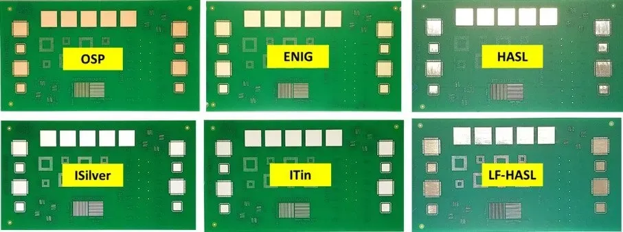
    Surface Finish Selection on FR4 Boards

    Surface finish is the last coating on exposed copper pads and holes. Bare copper oxidizes in air and becomes hard to solder, so the fabricator covers it before the board leaves the shop. On FR4 work the common choices are lead-free HASL, OSP, ENIG, immersion silver, and ENEPIG. Immersion tin is used less often on multilayer lead-free boards. The finish decides pad flatness, shelf life, how many reflow cycles the board can take, and whether a fine-pitch BGA will sit flat. It does not change the laminate. A wrong Tg still cracks vias after ENIG is applied.

    The table below compares those five production finishes. Use it to match pitch, assembly profile, and inventory time, not to repair a material grade that was specified too low.

    Surface Finish Comparison Table

    Finish

    Flatness

    Shelf life

    Reflow cycles

    Fine-pitch/BGA

    Cost

    Watch-outs

    LF HASL

    Poor–fair

    6–12 months

    Good

    Weak below ~0.5 mm pitch

    Low

    Uneven pads, not for fine BGA

    OSP

    Excellent

    3–6 months

    Limited

    Good if assembled soon

    Lowest

    Short window, handling, bake

    ENIG

    Excellent

    12+ months

    Good

    Excellent

    Mid

    Black pad if Ni/Au out of control

    Immersion Ag

    Excellent

    6–12 months

    Good

    Good

    Low–mid

    Tarnish, sulfur, handling

    ENEPIG

    Excellent

    12–24 months

    Excellent

    Excellent + wire bond

    High

    Cost; over-specified on simple boards

    FR4 Compliance and Material Certification

    On an FR4 board, compliance usually means the metals and organics in the laminate, copper, soldermask, and surface finish. It does not mean the board will survive reflow, and it does not replace a Tg or Td callout. Buyers still mix three different asks: substance limits (RoHS, REACH SVHC), halogen-free OEM rules, and factory papers such as UL or a Certificate of Compliance.

    For standard FR4 PCB production, RoHS-capable materials and finishes are commonly available, but the exact compliance package depends on the laminate, finish, and customer requirements.

    Halogen-free FR4 is a separate OEM request. It is not automatic on a standard RoHS board. UL 94 V-0 and a UL yellow card attach to a specific laminate construction, not to the letters FR4. If the end customer needs halogen-free, a named UL construction, or a later SVHC list than the published reports, say so before the order is placed.FR4 Compliance

    For a normal FR4 job, pick OSP, lead-free HASL, or ENIG on the quote. Those three finishes are the ones covered by the published SGS RoHS and REACH reports. No extra form is required for standard substance compliance.

    How to Select the Right FR4 Material

    The conversion question is simple: which FR4 should this board use? Rank criteria by risk, not by the order of datasheet pages.

    1.  Assembly chemistry and reflow count: leaded vs lead-free; single vs double-sided vs rework

    2.  Layer count and sequential lamination/HDI

    3.  Max continuous operating temperature and thermal cycling

    4.  Reliability class: IPC Class 2 vs 3, automotive, industrial, medical

    5.  Electrical: impedance tolerance, bit rate, and when to leave commodity FR4 for enhanced-electrical or mid-loss

    6.  Environment/OEM halogen and substance rules

    7.  Volume, lead time, and approved-vendor list

    Application-Based Quick Picks

    Application

    Typical pick

    Consumer IoT, LED, 2–4 layer

    Standard or mid-Tg + HASL or OSP

    Industrial control, 4–8 layer lead-free

    Mid- or high-Tg + ENIG

    Automotive ECU / power

    High-Tg, CAF-capable, IATF supply chain + ENIG or ENEPIG

    Server / multilayer backplane

    High-Tg low-CTE, Td ≥340 °C

    Medical / regulated consumer

    High-Tg or HF high-Tg + full RoHS/REACH pack

    High-voltage

    CTI-rated FR4 and creepage rules, not a Tg-only choice

    CEZON FR4 Manufacturing Experience

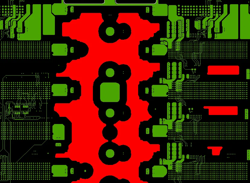
    CEZON builds routine stackups from stock material: FR4, TG150, halogenated resin. That grade is the everyday mid-Tg choice for lead-free 2–8 layer work. It does not correct a one-sided copper pour. When residual copper on TL and BL differs too much, bow and twist are hard to hold to the shop limit of ≤0.75%. CAM then adds balance copper in the blank areas on the sparse side, 6 mm away from traces, pads, and drilled holes. On the markup, that copper is shown in red.

    FR4 Manufacturing Case

    Why is FR4 particularly sensitive to copper distribution imbalances?

    FR4 consists of fiberglass cloth and epoxy resin with copper cladding. During manufacturing, the board undergoes lamination, drilling and plating, and lead-free reflow soldering. During each heating cycle, the resin softens as it passes the glass transition temperature; the difference in thermal expansion between the copper and the dielectric material pulls the board toward the side with less copper.

    This effect is more pronounced in boards with fewer layers or thinner profiles. For 2-layer or 4-layer boards, the top and bottom layers face each other directly without internal planes to provide structural support. Even with 8 or more layers, if the copper distribution between inner and outer layers is asymmetrical, warping will still exceed limits. High-Tg materials only shorten the window of time during which the resin remains soft; they cannot compensate for a disparity in copper surface area.

    Therefore, material selection addresses the risk of delamination during reflow, while copper pouring addresses the risk of board bending. High-Tg or ENIG will not flatten that panel. Symmetry will. Keep top and bottom residual copper close in the layout, or allow the 6 mm clearance pour on the empty face and on the breakaway tab. If a face must stay empty for assembly, say so on the note so the red pour is not added by default.

    Conclusion

    The most important lesson in FR4 selection is simple: FR4 is a starting material category, not a complete engineering specification.

    A manufacturable PCB specification should identify the laminate grade or approved family, Tg and Td, relevant CTE behavior, IPC-4101 classification, electrical requirements, copper construction, surface finish, and compliance requirements.

    The right material decision also depends on the fabrication process. Lamination, drilling, desmear, plating, solder mask, and surface finish all respond to material characteristics. A material change should therefore trigger a manufacturing review rather than being treated as a purchasing-only substitution.

    FAQs

    Q1: What is the difference between FR4 TG130, TG150, and TG170?

    A1: TG130 is a standard FR4 grade with a glass transition temperature around 130–140 °C by DSC, while TG150 provides a higher thermal margin and is commonly used for lead-free multilayer boards. TG170 combines a higher Tg with properties such as higher decomposition temperature (Td), lower Z-axis thermal expansion, and longer T-288 resistance. When selecting FR4, compare actual Tg, Td, CTE, and T-288 data rather than relying only on the material grade name.

    Q2: Is standard FR4 compatible with lead-free (RoHS) soldering?

    A2: Standard FR4 can sometimes withstand a single moderate lead-free soldering profile, particularly on simple two-layer boards. Multilayer boards, repeated reflow, and rework require greater thermal reliability, so Td and T-288 should be evaluated in addition to Tg. RoHS-compliant solder alloy does not by itself improve the thermal performance of the laminate.

    Q3: Does halogen-free FR4 perform the same as standard FR4?

    A3: Halogen-free FR4 can achieve the same UL 94 V-0 flame rating as conventional FR4, but other material and processing characteristics may differ. Moisture behavior, processing window, drilling and desmear performance, and cost can vary by material system. When halogen-free construction is required, material-specific bake and humidity controls should be established.

    Q4: Which surface finish is best on FR4 for BGA and multiple reflow?

    A4: ENIG and ENEPIG are commonly selected for BGA applications because they provide a relatively flat surface and good solderability through multiple assembly cycles. OSP can also be suitable when inventory turnover and storage conditions are tightly controlled. Lead-free HASL may be less suitable for fine-pitch BGA because its surface height variation is generally greater than that of planar finishes.

    Q5: Why did my FR4 board warp or delaminate after assembly?

    A5: Common causes include insufficient laminate thermal performance for the assembly profile, excessive moisture, an asymmetric stack-up, incomplete press curing, and unbalanced copper distribution. These factors can create thermal stress and dimensional changes during reflow. Solder paste itself is usually not the first factor to investigate when diagnosing FR4 warpage or delamination.

    Get in Touch