


FPC Design Rules: The Complete Guide to Reliable Flexible PCB Design

Core Knowledge and Engineering Practices for FPC Design

Flexible printed circuits (FPCs) consist of thin, bendable substrates with conductive traces that enable compact, three-dimensional electronic packaging. Unlike rigid PCBs built on FR4 or similar laminates, FPCs use polymer films such as polyimide (PI) or polyester (PET) that allow repeated flexing or static forming. Key advantages include reduced weight and thickness, the ability to fit into tight or moving assemblies, and support for high-density interconnects without bulky connectors or cables. These characteristics make FPCs essential in space-constrained or motion-intensive applications.

Engineers distinguish between static bend and dynamic flex PCB applications. Static designs involve a one-time or occasional bend during assembly or installation, while dynamic flex requires repeated bending over the product lifetime, often tens of thousands to millions of cycles. The difference drives entirely different material and layout choices.

Industry demand comes from consumer electronics like foldable phones and smartwatches, automotive systems including dashboard displays and sensor harnesses, medical devices such as endoscopes and wearable monitors, aerospace avionics, and industrial automation. In each sector, poor FPC design leads to field failures, warranty claims, and delayed time-to-market.

This guide compiles practical design rules drawn from factory CAM experience, DFM reviews, and reliability testing. It covers material selection, bend region optimization, impedance control, application-specific considerations, and real production cases. Following these guidelines helps reduce defect rates, improve yields, and streamline RFQ processes for both designers and manufacturers.

Material Selection as the Foundation of FPC Design

Material selection is one of the earliest and most critical decisions in flexible circuit design. Unlike rigid PCBs, the mechanical performance, bend reliability, thermal resistance, and manufacturing cost of an FPC are heavily influenced by the material system chosen before layout begins. An inappropriate material choice can lead to premature fatigue failures, delamination, impedance instability, or assembly defects regardless of how well the circuit is routed.

Substrate Material Selection: PI vs PET

Property

Polyimide (PI)

Polyester (PET)

Temperature Resistance

Excellent (>300°C thermal stability)

Limited temperature resistance

Flexibility

Excellent

Good

Dimensional Stability

Excellent

Moderate

Reflow Soldering Compatibility

Suitable

Generally unsuitable

Reliability

High

Moderate

Typical Applications

Automotive, aerospace, industrial, medical electronics

Consumer electronics, low-cost products

Cost

Higher

Lower

Recommended For

High-reliability and demanding environments

Cost-sensitive static applications

PI remains the dominant substrate material for professional FPC designs because it combines thermal stability, mechanical durability, and long-term reliability. PET is primarily used when cost reduction outweighs performance requirements.

Polyimide is widely used in demanding flexible circuits because it offers good thermal stability, dimensional stability, and flexibility. It is suitable for applications that involve repeated bending, higher operating temperatures, or more demanding assembly processes.

Polyester, commonly known as PET, may be suitable for simpler and more cost-sensitive flexible circuits. It is often used in applications where the circuit has limited movement and does not need to withstand high-temperature processing.

The substrate should be selected according to the actual application rather than price alone. Designers should review operating temperature, bend requirements, dielectric performance, and assembly conditions before choosing the material.

Copper Foil Selection: RA vs ED Copper

Property

Rolled Annealed (RA) Copper

Electrodeposited (ED) Copper

Grain Structure

Horizontal elongated grains

Vertical columnar grains

Ductility

Excellent

Moderate

Dynamic Flex Performance

Excellent

Limited

Fatigue Resistance

High

Lower

Repeated Bend Cycles

Suitable

Not recommended

Static Flex Applications

Suitable

Suitable

Cost

Higher

Lower

Recommended For

Dynamic flex circuits and high-cycle bending

Static flex and cost-sensitive designs

Copper type is another important consideration in FPC design.

Dynamic flex circuits should generally use RA copper because its grain structure better withstands cyclic mechanical stress. While ED copper is widely used in static flex applications, repeated bending can accelerate fatigue cracking and reduce service life.

Designers must also evaluate whether to use adhesive-based or adhesiveless constructions. Adhesiveless laminates bond copper directly to the polyimide film, reducing overall thickness while improving thermal performance and bend life. These constructions are commonly recommended for high-density designs and dynamic flex regions. Adhesive-based materials remain widely used in cost-sensitive applications but typically exhibit lower long-term flex reliability.

Coverlay, Adhesive, and Stiffener Selection

Coverlay protects the copper traces and provides electrical insulation. Its thickness and opening design affect flexibility, bend performance, pad access, and assembly.

Adhesive-based and adhesiveless constructions may have different mechanical and dimensional characteristics. Designers should confirm which construction is suitable for the intended application.

Stiffeners are often added beneath connectors, component areas, or contact pads. They improve local support and help prevent damage during assembly or insertion. However, stiffeners also increase local thickness and may affect the bend transition.

In flexible PCB design, stiffeners should be placed only where mechanical reinforcement is needed. The transition between stiffened and flexible areas should be designed smoothly to avoid concentrated stress.

FPC Design Fundamental Rules

The main FPC design rules focus on controlling mechanical stress, protecting conductors, and maintaining manufacturable geometry. A flex circuit should not be treated as a rigid PCB that is simply made thinner.

Basic Layout Rules

Basic layout rules form the foundation of manufacturable and reliable FPC designs. Minimum trace width and spacing are typically 75 µm-100 µm for standard production volumes, with advanced processes supporting 50 µm or finer in prototype quantities. These limits depend heavily on copper thickness and chosen fabricator capabilities, so always confirm with your manufacturer rather than assuming generic values. In high-current areas, widen traces or use copper pours while maintaining flexibility; in signal layers, control impedance by adjusting width and reference plane distance.

Trace routing in flex areas should prioritize straight runs perpendicular to the bend axis to minimize strain. When perpendicular routing is impossible, use gentle arcs with radius at least 2× trace width. Stagger traces in differential pairs or multi-layer bundles to prevent overlapping stress points during repeated bending. Implement teardrops on all pads (minimum 50% extension) to strengthen the trace-pad junction and compensate for registration tolerances. All trace corners must use a minimum 45° chamfer or full radius — sharp 90° corners act as stress concentrators and frequently initiate copper cracks under dynamic flex.

Component pads in flex zones should be reinforced with local stiffeners, and keep large components or connectors away from bend areas. Proper Flexible PCB connector design is also important when the circuit uses an FPC ZIF connector, as interface selection, contact geometry, ZIF vs LIF requirements, and Gold finger design can all affect assembly reliability. Fiducials for assembly and inspection must be placed in rigid or semi-rigid zones with sufficient clearance. Panelization features such as mouse bites, stamp holes, or V-scores require careful positioning to avoid interfering with functional flexing areas. Following these rules consistently prevents common issues like trace fracturing, pad lifting, and registration-related defects during lamination and coverlay application.

Stack-up design principles

The stack-up determines the overall thickness, flexibility, electrical performance, and mechanical behavior of a flexible circuit. A suitable flexible PCB stack-up design should balance copper distribution, dielectric thickness, coverlay, adhesive, and reinforcement.

Single-layer flexible circuits are often used for simple routing, lightweight interconnects, and applications with limited electrical complexity. They generally provide good flexibility and can be easier to manufacture.

Double-layer flexible circuits provide more routing space and may support better grounding or signal distribution. However, the additional copper and dielectric layers increase total thickness and may reduce bend flexibility.


Multilayer flexible PCB design is useful when the circuit requires higher routing density, controlled impedance, shielding, or more complex interconnections.

However, additional layers increase the total thickness and can make the circuit less flexible. The stack-up should therefore be designed around the actual mechanical requirements.

Key principles include placing critical high-speed signals on inner layers when possible for better protection, using adhesiveless materials for thinner profiles and superior flex life, and carefully managing dielectric thicknesses for impedance targets. In rigid-flex designs, transition zones should gradually change layer count and stiffness with stepped or tapered copper removal to avoid abrupt stress changes that cause delamination.

Flexible PCB copper thickness selection follows a clear tradeoff: 12 µm or 18 µm for high-flex applications, 35 µm or heavier for power distribution. FPC copper thinning can help reduce bending strain in demanding flex areas, but the final design must still balance Flexible PCB trace width, current-carrying requirements, and copper thickness impedance. Total stack thickness in dynamic bend areas should stay below 0.15–0.25 mm for optimal performance. Always simulate the complete stack-up for both electrical (impedance, crosstalk) and mechanical (bend stress) performance. Unbalanced or overly thick stack-ups commonly cause warpage, coverlay wrinkling, or reduced flex endurance that only becomes evident after environmental testing.

Grounding and Shielding Strategies

Effective grounding and shielding are essential for maintaining signal integrity and EMI/EMC performance in FPC designs, particularly in high-speed or noise-sensitive applications. In flexible circuits, ground planes should be implemented as continuous copper pours on one or both sides of signal layers whenever possible, with strategic cross-hatching only when full planes would excessively reduce flexibility.

Solid ground planes provide the best return paths and shielding but increase stiffness; hatched patterns (typically 45-60% copper coverage) offer a compromise for dynamic flex zones while still controlling impedance and reducing crosstalk.

Stitching vias or conductive adhesive between ground layers in multilayer FPCs ensure low-impedance connections across the stack-up. In bend areas, avoid breaking ground continuity—route ground traces or planes to follow the neutral bend axis where mechanical strain is minimal.

For EMI shielding, consider additional silver ink shielding layers, copper foil tapes, or dedicated shield films bonded to the coverlay, especially in wearable and medical devices where external interference or patient safety is critical. Always verify shielding effectiveness through radiated emission testing and maintain ground return paths as short and wide as possible to minimize loop inductance. Poor grounding frequently leads to signal noise, radiated emissions failures, or ground bounce issues that only appear during system-level integration.

Via and Pad Design Guidelines

Via and pad design in FPCs requires special attention due to the mechanical stresses unique to flexible materials. Use teardrop pads at all trace-to-pad junctions to prevent trace necking and pad lifting during bending or thermal expansion.

Minimum annular ring is typically 0.075-0.1mm for reliable plating, with larger rings (0.15 mm+) recommended in high-reliability or dynamic applications.

Plated through holes (PTH) should maintain a hole-to-pad ratio that accounts for drill wander and registration tolerances common in flex processing. Blind and buried vias improve density in multilayer designs but increase cost and require careful aspect ratio control.

Never place vias directly in dynamic bend zones, as the plating barrel experiences high strain and cracks easily. If vias are unavoidable near bend areas, position them in reinforced static regions and add extra coverlay or stiffener support. Pad shapes should favor rounded or oblong geometries in flex zones to distribute stress. During DFM review, check for via tenting consistency and solder mask or coverlay clearance to avoid solder wicking or shorting risks.

Ignoring these guidelines commonly results in annular ring breakout, via barrel fractures under flexing, or assembly defects that reduce yield and long-term reliability. In production, cross-section analysis of vias is a standard validation step to confirm plating quality before committing to volume.

Bend Area Design Principles

The bend area is the highest-risk zone in most FPC designs. Proper FPC bend radius selection and Flexible PCB stress relief directly determine whether the circuit will survive its intended lifetime or fail prematurely in the field.

Static vs Dynamic Bend Requirements

For static bend applications, where the FPC is bent once during assembly or installation and remains in a fixed shape, the minimum bend radius is typically 6 to 10 times the total circuit thickness. This is relatively forgiving and allows more compact designs.

For dynamic flex applications, such as foldable wearables, hinge mechanisms, or sliding assemblies that experience repeated bending, the requirements are much stricter. Recommended bend radii are often 100 times the total thickness or greater, depending on the required cycle life. A design targeting hundreds of thousands of cycles may need a noticeably larger radius than one intended for only a few thousand movements.

In practice, we evaluate the bend radius together with the overall stack thickness, copper type, and application environment during DFM reviews. Overly aggressive (too small) bend radii are one of the most common causes of early field failures.

Designing Smooth Bend Transitions

In FPC design, smooth transitions are critical in areas where the circuit changes from a flat section to a bend zone, or where local stiffness varies due to coverlay, copper thickness, or stiffener placement. Poorly designed transitions often become stress concentration points and lead to copper cracking or delamination over time.

Key Considerations for Smooth Bend Transitions:

● Gradual Change in Stiffness: Avoid abrupt changes in the stack-up or coverlay at the start and end of bend areas. Use tapered coverlay edges or gradually adjust copper density to create a smoother mechanical transition.

● Transition Zone Length: Provide enough length between the flat area and the actual bend radius. A short or sharp transition increases localized stress. In most cases, a transition zone of several millimeters helps distribute strain more evenly.

● Trace and Feature Management: Keep critical traces, vias, and pads away from transition boundaries. Route traces perpendicular to the transition line when possible, and avoid sudden width changes near the bend entry point.Strain Relief Features: Add tear stops, rounded corners, or slight relief slots at transition edges to prevent tears from initiating and propagating into functional areas.

● Coverlay and Copper Optimization: In high-cycle applications, consider slightly thicker coverlay or localized reinforcement in transition zones to improve durability without overly restricting flexibility.

When laying out FPCs, always define clear bend zones and transition zones in the mechanical layers. During DFM review, check whether the transition from flat to bend is too abrupt. For demanding dynamic applications, it is recommended to validate the transition design through prototype bending tests, as simulation alone often underestimates the stress at these boundary areas.

Well-executed bend transitions significantly improve the long-term reliability of flexible circuits, especially in products that require repeated flexing.

Impedance Control in Flexible PCB Design

Impedance control in flexible circuits is more challenging than on rigid boards because the materials and geometry can change during bending and manufacturing. Several key factors directly influence impedance in FPC designs:

Main Factors Affecting Impedance Control:

Factor

Description

Impact on Impedance

Design Consideration

Dielectric Thickness

Thickness of substrate and coverlay

Directly affects characteristic impedance

Control coverlay thickness tolerance tightly

Coverlay & Adhesive

Coverlay material, thickness, and adhesive flow during lamination

Can shift impedance by 5–10%

Specify tight coverlay tolerances; validate with TDR

Trace Geometry

Trace width, spacing, and copper thickness

Determines target impedance value

Adjust trace width according to copper thickness and target Zo

Configuration Type

Microstrip (outer layer) vs Stripline (inner layer)

Different behavior due to dielectric environment

Choose configuration based on layer and shielding needs

Bend Area Effects

Stretching or compression of substrate during bending

Changes differential pair spacing

Maintain consistent spacing; avoid critical signals in tight bend zones

Material Variation

Variations in dielectric constant and copper thickness

Causes deviation between simulation and actual

Correlate simulation with prototype TDR measurements

Practical Recommendations

Because of these variables, simulation tools (such as HyperLynx or SIwave) provide a good starting point but are not sufficient by themselves. In real FPC production, coverlay thickness variation and adhesive flow often cause the actual impedance to deviate from simulation results.

For critical designs, it is recommended to:

● Define clear impedance requirements early in the stack-up stage

● Run simulation and then validate with TDR testing on prototypes

● Work closely with the fabricator to confirm achievable tolerances on coverlay and dielectric thickness

● This approach helps achieve more reliable and repeatable impedance control in flexible printed circuits.

FPC Design Guidelines for DFM and Manufacturing

A practical CAD workflow for FPC starts with importing accurate mechanical constraints and clearly marking all bend zones, fold lines, and stiffener locations as mechanical layers. Define flex-specific design rules early for trace width, spacing, annular rings, and keep-out areas. After routing and stack-up finalization, the most critical phase begins: a thorough DFM review. This final checkpoint determines whether the design will move smoothly into production or require costly iterations.

Flex PCB DFM Checklist:

Item

Requirement

Typical Tolerance/Note

Trace Width / Spacing

75 µm — 100 µm

Confirm with fabricator capability

Annular Ring

≥0.1 mm

0.15 mm preferred for dynamic areas

Teardrops

Required on all pads

Minimum 50% extension

Bend Radius

Static: 6–10× thickness

Dynamic: ≥100× thickness

Validate with target cycle count

Via Placement

No vias in dynamic bend zones

Allowed only in reinforced static areas

Coverlay Registration

±0.075–0.1 mm

Critical for exposed traces

Panelization

Fiducials, tooling holes, mouse bites

Avoid interfering with flex areas

Impedance Control

±10% target

Document required layers and structures

Stiffener Alignment

±0.1 mm

Adhesive flow control

This structured final checkpoint, aligned with IPC standards, has proven to be the most effective way to catch issues that would otherwise surface only after fabrication or during reliability testing. Following this process consistently helps achieve higher first-pass yield and shorter overall development time.

IPC Standards for Flexible Circuit Design

Standard

Purpose

Key Relevance to FPC Design

IPC-2223

Design Standard for Flexible Printed Boards

Bend area rules, stack-up guidelines, material selection

IPC-6013

Qualification and Performance Specification for Flexible Printed Boards

Acceptance criteria, reliability test methods

IPC-TM-650

Test Methods Manual

Dynamic bend testing, thermal stress, solderability

IPC-2221

Generic Standard on Printed Board Design

General requirements (used in conjunction with 2223)

IPC-6012

Qualification for Rigid Boards

Applicable to rigid portions of rigid-flex designs

Flexible PCB Design for Different Applications

Wearable Flexible PCB Design

Wearable devices demand ultra-thin profiles, skin conformability, and sweat resistance. Flexible PCB for wearable electronics must also support high-density layouts with fine-pitch traces and multiple sensors. Material selection often favors thin RA copper on PI with specialized coverlays or soldermask alternatives to maintain flexibility. Dynamic bending occurs around the wrist or joint areas, requiring careful bend-radius control and trace routing.

Automotive Flexible Circuit Design

The Automotive multilayer flexible PCB faces wide temperature ranges, vibration, and AEC-Q100/200 qualification. Designs incorporate thicker copper for current carrying in power distribution or high-reliability materials for sensors and cameras. Vibration-resistant stiffeners and redundant traces improve robustness. Manufacturing must include enhanced thermal cycling and vibration testing.

Medical Flexible PCB Design

Medical FPCs prioritize biocompatibility, miniaturization, and sterilization compatibility. Single-use devices favor cost-optimized constructions, while reusable ones need robust dynamic performance. ISO 10993 and other standards apply. Miniaturization pushes via and trace limits, making DFM collaboration with the manufacturer essential early in development.

Manufacturing practices

Roll-to-roll (R2R) processing enables high-volume, cost-effective production for simpler designs. Laser drilling, precise coverlay alignment, and automated stiffener attachment are critical. Impedance testing, AOI, X-ray, and sample bend testing form part of quality controls. Electrical testing under flex conditions is increasingly common for dynamic applications.

Process choices affect yield-cost balance. Early DFM collaboration with the fabricator prevents costly iterations.

Common FPC Design Mistakes and How to Avoid Them

Mistake

Root Cause

Risk

Consequence

Recommended Fix

Placing vias or pads in bend zones

Overlooking mechanical stress in layout

High stress concentration

Via cracking, trace fracture, open circuits

Keep bend areas free of vias/pads; route traces perpendicular to bend

Using ED copper in high-cycle dynamic applications

Cost-driven material selection without flex life analysis

Rapid fatigue

Early field failures

Specify RA copper for dynamic zones; validate with IPC-TM-650 testing

Insufficient bend radius

CAD looks fine but ignores total stack thickness

Copper strain exceeds limits

Cracking after limited cycles

Apply 6-10× for static, ≥100× guideline for dynamic; calculate per construction

Sharp trace corners or no teardrops

Ignoring stress risers

Localized cracking

Intermittent opens or shorts

Always use rounded corners and teardrops

Poor rigid-flex transition design

Abrupt mechanical and impedance changes

Delamination, impedance mismatch

Signal integrity failures

Gradual transitions, reinforcement, simulation validation

Ignoring coverlay registration tolerances

Assuming perfect alignment

Exposed traces or shorts

Yield loss, reliability issues

Add generous tolerances and review with manufacturer

Inadequate stiffener placement

Component mounting without support

Solder joint fatigue

Broken connections

Place stiffeners under all heavy components

Skipping TDR validation

Relying solely on simulation

Undetected discontinuities

System-level signal problems

Perform TDR on prototypes and production samples

Conclusion

Effective FPC design balances electrical performance, mechanical reliability, and manufacturability. The bend region remains the critical failure zone in most applications—get the radius, material, and routing correct and you avoid the majority of problems. Material selection, especially copper type and construction method, determines whether your product survives qualification or reaches the field only to return under warranty.

Real manufacturing data shows that designs developed in close collaboration with experienced fabricators achieve higher yields and faster ramps to volume. Early DFM reviews catch issues that CAD tools alone miss.

For your next project, consider submitting files for a complimentary DFM review. Our engineering team can provide stack-up recommendations, bend optimization, and impedance modeling tailored to your application.

FPC Design Frequently Asked Questions

Q1: How is minimum dynamic bend radius calculated for FPC?

A1: Use total circuit thickness multiplied by a factor derived from required cycle life, copper thickness, and material. Consult manufacturer-specific tables or run IPC-TM-650 testing. A common empirical rule is radius ≥ 100 × total thickness for high-cycle applications, adjusted by material data and testing. Use finite element modeling for complex geometries and always validate with physical samples.

Q2: What are the differences between RA and ED copper in flex applications?

A2: RA copper offers superior ductility and fatigue resistance due to its aligned grain structure. ED copper is cheaper and sufficient for static or low-cycle use but shows earlier crack initiation under repeated strain. Choose RA for any dynamic requirement exceeding a few thousand cycles.

Q3: How to achieve 50Ω/100Ω impedance control in FPC?

A3: Control dielectric thickness, trace width/spacing, and reference plane proximity tightly. Use simulation tools, specify tight tolerances on coverlay, and verify with TDR. Adhesiveless constructions provide more predictable results.

Q4: What failures result from common mistakes like sharp trace corners or missing teardrops?

A4: Stress risers initiate cracks that propagate through copper, causing opens. Missing teardrops lead to pad lifting or trace breakout, especially during flex or thermal stress.

Q5: How to choose between FPC and Rigid-Flex?

A5: Choose pure FPC for cost efficiency and simple designs when dynamic flex or tight packaging is needed without dense components on the flexible portion. Choose Rigid-Flex when components must reside on the flexible part or when multiple rigid sections are required.

Q6: What special certifications are required for medical/automotive FPC?

A6: Automotive FPCs require IATF 16949 quality management systems, ISO 26262 functional safety standards, AEC-Q100/200 series standards, and application-specific reliability testing. Medical FPCs typically require ISO 13485 manufacturing controls and biocompatibility compliance per ISO 10993. Both applications require detailed process validation and traceability.

Q7: What are the basic rules for flexible PCB design?

A7: The basic rules for flexible PCB design include selecting suitable materials, defining bend zones, using smooth trace routing, avoiding sharp corners, keeping vias and large components away from dynamic bend areas, and confirming trace width, spacing, coverlay clearance, and stack-up requirements with the manufacturer.

Q8: What is the difference between FPC design and rigid PCB design?

A8: FPC design must consider both electrical and mechanical behavior. Unlike rigid PCB design, flexible circuits may bend, twist, or move during operation. Designers therefore need to evaluate bend radius, copper type, substrate thickness, coverlay, stiffeners, and transition zones in addition to standard layout requirements.

Q9: How do you design a flex PCB?

A9: To design a flex PCB, first define the mechanical envelope, bend zones, and electrical requirements. Then select the substrate, copper type, coverlay, and stiffeners. During layout, use smooth trace paths, avoid placing vias in dynamic bend areas, provide a suitable bend radius, and review the complete stack-up. A flex PCB design DFM review should be completed before fabrication.

Q10: What is the recommended bend radius for a flexible PCB?

A10: The recommended bend radius depends on the total circuit thickness, copper type, material construction, bend direction, and expected bending cycles. Static-bend applications generally allow a tighter radius than dynamic-flex applications. For repeated bending, designers should use construction-specific guidance from the manufacturer and validate the design through mechanical testing.

Q11: Can vias be placed in a flexible PCB bend area?

A11: Vias should generally be kept out of demanding dynamic bend areas because the plated structure can experience repeated mechanical strain. If a via must be placed near a bend, it should be located in a relatively stable or reinforced area with suitable clearance and mechanical support.

Q12: How does copper thickness affect flexible PCB design?

A12: Copper thickness affects flexibility, trace width, current-carrying capacity, impedance, and manufacturing capability. Thinner copper may improve bend performance and fine-line routing, while thicker copper can support higher current. The final choice should balance electrical requirements with total stack thickness, bend radius, copper type, and reliability expectations.

Q13: What materials are commonly used in FPC design?

A13: Common materials used in FPC design include polyimide, polyester, rolled-annealed copper, electrodeposited copper, coverlay, adhesives, and stiffeners. Polyimide and RA copper are often selected for demanding flexible applications, while PET and ED copper may be suitable for certain static or cost-sensitive designs.

Q14: What is the role of DFM in flexible PCB design?

A14: DFM helps verify whether a flexible circuit can be manufactured consistently. An FPC DFM review normally checks trace width and spacing, copper-to-edge clearance, coverlay registration, bend-zone layout, via placement, stiffener alignment, panelization, stack-up thickness, and assembly requirements.

Q15: What standards are used for flexible circuit board design?

A15: IPC-2223 is commonly referenced for flexible printed board design, while IPC-6013 covers qualification and performance requirements for flexible circuits. Relevant IPC test methods may also be used to evaluate material, plating, electrical, and mechanical performance. The applicable requirements should be selected according to the product, material construction, reliability target, and customer specification.

Get in Touch


    Complete Guide to FPC Materials and Flexible PCB Manufacturing

    Flexible PCB manufacturing plays an important role in modern electronic systems where traditional rigid PCBs cannot provide the required flexibility, compactness, or three-dimensional routing. Flexible printed circuits are widely used in automotive electronics, medical devices, aerospace systems, wearable products, and consumer electronics.

    Successful flex PCB fabrication depends on more than the circuit layout. Substrate selection, copper foil type, coverlay, adhesive systems, surface finish, and manufacturing controls all affect the final performance of an FPC. These factors influence flexibility, thermal stability, signal integrity, environmental resistance, and long-term reliability.

    This guide explains the key FPC materials, manufacturing processes, common failure modes, and material selection considerations for different applications. It also outlines how engineers can evaluate flexible circuit designs and work with an experienced manufacturer to achieve consistent production results.

    Understanding Flexible Printed Circuits and the Critical Role of Materials

    What Is an FPC?

    FPC stands for Flexible Printed Circuit. It is a printed circuit board built on a flexible substrate instead of a rigid material. This structure allows the circuit to bend, fold, or fit into compact spaces while maintaining electrical connections between components.

    FPCs are commonly used where space, weight, and mechanical flexibility are important. Typical applications include displays, cameras, battery connections, medical devices, automotive electronics, wearable products, and industrial equipment.

    Material choices influence nearly every key performance metric:

    ● Mechanical flexibility and fatigue life: Determines how many bend cycles the circuit can endure.

    ● Thermal performance: Affects solderability, operating temperature range, and resistance to reflow processes.

    ● Electrical characteristics: Impacts impedance control, signal loss, and high-frequency performance.

    ● Environmental resistance: Influences moisture absorption, chemical compatibility, and outgassing behavior.

    ● Manufacturing yield and cost: Directly affects production economics and scalability.

    In high-reliability sectors such as automotive (under-hood electronics), medical (implantable or reusable devices), and aerospace (vibration-intensive environments), suboptimal material selection often leads to field failures that carry substantial warranty and safety implications.

    How Are Flexible PCBs Different from Rigid PCBs?

    The main difference is the substrate and the mechanical behavior of the finished board.

    Rigid PCBs usually use materials such as FR-4, which provide a stable and solid structure. Flexible PCBs use materials such as polyimide or polyester, allowing the circuit to bend and conform to the product structure.

    Compared with rigid PCBs, flexible circuits can offer:

    • Better space utilization

    • Lower assembly weight

    • Fewer connectors and solder joints

    • Easier three-dimensional routing

    • Better suitability for moving or bending applications

    However, flexible circuits require careful control of bend areas, copper layout, coverlay design, and material selection during flexible PCB manufacturing.

    Key Materials Used in Flexible PCB Manufacturing

    Polyimide and Other Flexible Substrate Materials

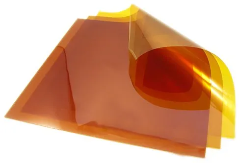
    Polyimide (PI) films represent the gold standard for demanding FPC applications. These aromatic polymers offer exceptional thermal stability with continuous service temperatures reaching 260°C and short-term tolerance exceeding 300°C during lead-free soldering. Their low coefficient of thermal expansion closely matches copper, minimizing stress during thermal cycling.

    PI films exhibit excellent tensile strength, high elongation before break, and superior dielectric properties. When properly engineered, PI-based FPCs can achieve dynamic flex life exceeding one million cycles. Major commercial grades such as DuPont Kapton or Kaneka Apical provide consistent performance across global supply chains.

    Polyimide film for flexible printed circuits

    Polyester and Other Cost-Effective Substrate Options

    Polyester (PET) films serve as a cost-effective option for less demanding applications. PET offers good electrical insulation and mechanical flexibility at significantly lower material costs — often 30-50% cheaper than PI. However, its limitations are notable: maximum continuous operating temperature usually ranges from 85°C to 150°C depending on grade, higher moisture absorption, and reduced long-term thermal stability. PET suits static flex-to-install designs in consumer electronics, such as display connections in smartphones or laptops, where extreme temperatures or dynamic motion are absent.

    PET substrates for FPC

    Advanced polymer options fill specific performance gaps:

    ● Polyethylene Naphthalate (PEN): Provides a middle ground with better thermal resistance than PET (up to 180°C) and improved dimensional stability.

    ● Liquid Crystal Polymer (LCP): Delivers ultra-low dielectric constant and dissipation factor, near-zero moisture absorption, and excellent high-frequency performance up to mmWave ranges. LCP excels in 5G antennas, radar modules, and high-speed data applications.

    ● PTFE (Polytetrafluoroethylene) composites: Offer superior chemical resistance and low dielectric loss for RF/microwave circuits, though they present unique processing challenges due to low surface energy.

    Comparative Analysis of Substrate Materials

    This table provides a comparison of common FPC base materials.

    Property

    Polyimide (PI)

    Polyester (PET)

    LCP

    PEN

    Max Operating Temp (°C)

    260+

    85-150

    200+

    150-180

    Moisture Absorption (%)

    1.3-3.0

    0.4-0.8

    <0.02

    0.2-0.4

    CTE (ppm/°C)

    20-30

    20-50

    10-20

    15-25

    Flex Life (Dynamic)

    Excellent (>1M cycles)

    Moderate

    Good

    Good

    Dielectric Constant

    3.4-3.5

    3.0-3.5

    2.9-3.0

    3.0-3.2

    Relative Cost

    High

    Low

    Very High

    Medium

    Typical Applications

    Automotive, Aerospace, Medical

    Consumer Electronics

    RF/5G, High-Speed

    Industrial Sensors

    Engineers must evaluate these properties against specific application requirements rather than selecting based solely on cost.

    Copper Foil Engineering: Rolled Annealed vs Electrodeposited

    While substrate materials form the mechanical and thermal foundation of an FPC, conductor performance is equally critical. In many dynamic flex applications, the copper layer experiences the highest mechanical stress during bending cycles. As a result, selecting the appropriate copper foil structure is often just as important as choosing the right dielectric material. Copper foil selection represents one of the most critical decisions in dynamic FPC design. Two primary types dominate the industry:

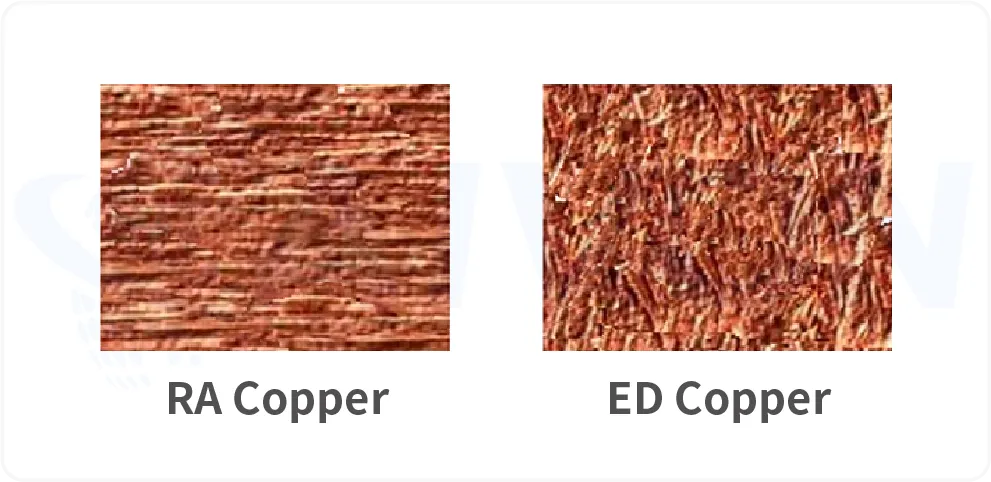
    Rolled Annealed (RA) Copper undergoes a mechanical rolling and annealing process that creates a smooth, elongated grain structure. This microstructure provides superior ductility and resistance to fatigue cracking. When the rolling direction aligns parallel to the primary bend axis, RA copper delivers exceptional flex endurance. Typical thicknesses range from 9μm to 35μm for fine-line applications. RA copper is the preferred choice for applications requiring repeated dynamic flexing, such as hinge connections in foldable devices or automotive camera modules.

    Electrodeposited (ED) Copper grows through electrochemical deposition, resulting in a more columnar grain structure with higher surface roughness on one side. This roughness improves adhesion to dielectrics but reduces ductility compared to RA. ED copper performs adequately in static flex or high-current applications and offers cost advantages, especially in thicker gauges (up to 70μm or more for power distribution).

    Surface treatment and grain orientation significantly affect performance. Reverse treat (RT) or low-profile foils improve etchability and high-frequency characteristics by reducing skin effect losses.

    Rolled annealed and electrodeposited copper foil for FPC fabrication

    Manufacturing and Material Selection Implications

    Copper foil selection directly influences downstream FPC fabrication performance, especially in lamination, etching, and bending reliability.

    ● Dynamic flex reliability: RA copper’s elongated grain structure improves resistance to micro-crack initiation during repeated flexing, making it more suitable for high-cycle bending structures.

    ● Lamination adhesion: ED copper’s naturally rougher surface enhances bonding strength with dielectric materials, improving peel strength in multilayer constructions.

    ● Etching precision: Lower-profile treated foils (reverse treated or very low profile ED/RA) improve line definition and reduce undercutting, which is critical for fine-feature circuits.

    ● Thickness and process trade-offs: Thicker ED copper improves current carrying capacity but increases etch difficulty and minimum line/space limitations, requiring tighter process control.

    However, conductor reliability depends on more than copper selection alone. Flexible circuits also require protective materials that shield traces from mechanical damage, moisture, and environmental contamination while preserving bendability. This role is fulfilled by the coverlay system.

    How Coverlay Selection Affects FPC Protection and Flexibility

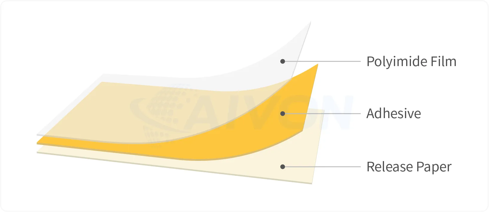
    FPC Coverlay is the primary protective layer for flexible circuits, replacing the solder mask used on rigid PCBs. It consists of a thin polymer film (usually PI or PET) coated with adhesive, providing mechanical support, electrical insulation, and environmental protection against dust, moisture, and chemicals.

    Coverlay structure used in flexible PCB manufacturing

    In production, coverlay thickness (typically 12.5μm, 25μm, or 50μm) creates important trade-offs. Thinner coverlays maximize flexibility and are preferred for tight bend radius applications, but they offer less abrasion resistance. Thicker coverlays improve durability and insulation reliability but can reduce overall circuit flexibility and increase stiffness in dynamic zones.

    Flexible PCB manufacturing process from material preparation to testing

    Material choice for coverlay should match the base substrate. PI coverlay paired with PI substrate provides the best thermal matching and long-term reliability in high-temperature or dynamic applications. PET coverlay is often used with PET substrates for cost-sensitive consumer products. The effectiveness of any coverlay system depends heavily on how it is bonded to the underlying circuit structure. Adhesive selection therefore becomes a key engineering consideration, influencing flexibility, thermal resistance, manufacturing yield, and long-term reliability.

    Adhesive Systems in FPC Production: Acrylic vs Epoxy Selection

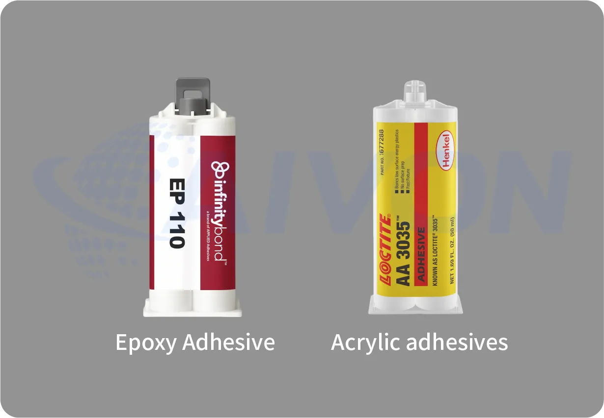
    Acrylic vs Epoxy Adhesive for FPC Production

    Adhesives serve as the bonding bridge between copper foil, substrate, and coverlay. They significantly influence manufacturing process windows, final mechanical properties, and long-term reliability.

    Acrylic adhesives offer excellent flexibility and are widely used in dynamic FPC production. They maintain good peel strength even after repeated bending and thermal aging. Acrylic systems are more forgiving during lamination, providing a wider process window and higher yields in high-flex applications.

    Epoxy adhesives deliver higher bond strength and superior high-temperature performance, making them suitable for automotive and aerospace production where thermal cycling is extreme. However, they are slightly more rigid and require tighter control of lamination temperature and pressure to prevent brittleness or delamination.

    Adhesiveless constructions are increasingly popular in high-performance manufacturing. By using plasma or chemical surface activation to bond copper directly to the dielectric, these structures eliminate adhesive layers entirely. Benefits include thinner overall thickness, better thermal conductivity, improved impedance control, and removal of adhesive-related failure modes. The trade-off is higher technical requirement in lamination equipment and process control.

    Manufacturing Impact Comparison:

    Adhesive Types

    Impact

    Acrylic

    Easier processing, better flexibility, moderate heat resistance.

    Epoxy

    Stronger bonding, higher thermal stability, narrower process window.

    Adhesiveless

    Best electrical and thermal performance, most demanding production controls

    Material and adhesive compatibility must be validated early, as mismatch is a leading cause of delamination during reflow or field use.

    Surface Finish Options for Flexible PCBs

    Once the internal material stack-up has been established, attention shifts to the exposed copper features that will ultimately be assembled and soldered. Surface finish selection plays a critical role in protecting these conductive areas while ensuring reliable electrical and mechanical connections throughout the product lifecycle. Surface finishes protect exposed copper pads and ensure reliable soldering or contact performance while maintaining circuit flexibility.

    Common options in FPC production:

    ● ENIG (Electroless Nickel Immersion Gold): Most popular for high-reliability applications. It offers excellent solderability, corrosion resistance, and wire-bonding capability. The nickel layer provides a hard barrier, while gold ensures long shelf life.

    ENIG Flexible PCB

    ● Immersion Silver (ImmAg): Cost-effective with good conductivity, suitable for high-frequency applications, but more sensitive to tarnishing and handling.

    ● OSP (Organic Solderability Preservative): Lowest cost, ideal for single-reflow consumer products, but limited shelf life and multiple reflow capability.

    OSP FPC

    ● Immersion Tin: Good for press-fit connectors but prone to whisker growth over time.

    Selection depends on assembly process, operating environment, and product lifecycle. For automotive and medical production, ENIG is often mandatory due to its reliability under thermal cycling and humidity exposure.

    In dynamic flex areas, the surface finish must not crack or flake during bending. Thinner finishes generally perform better for flexibility but may compromise long-term protection.

    Although material selection is fundamental, the final performance of an FPC depends equally on how those materials are processed. Even the best substrate, copper foil, and surface finish combinations can fail if manufacturing controls are not properly maintained. Understanding the fabrication process helps explain how material choices translate into real-world product reliability.

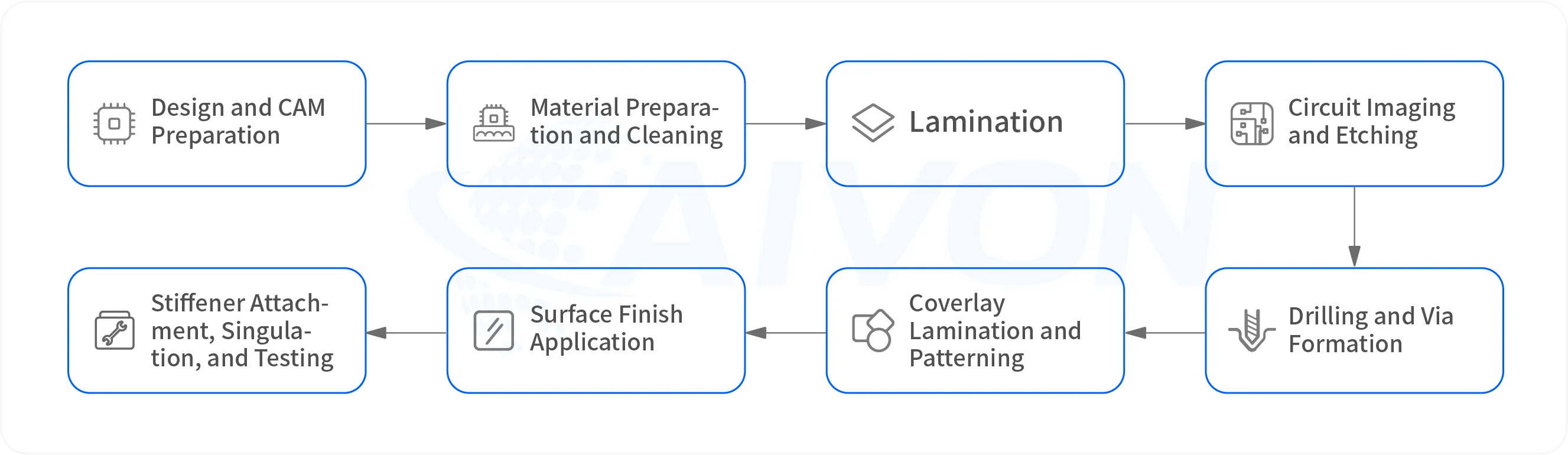
    Complete FPC Manufacturing Process and Quality Controls

    FPC fabrication involves specialized processes adapted to thin, flexible materials. Each step introduces variables that can affect final product reliability.

    Flexible PCB manufacturing process from material preparation to testing

    FPC Manufacturing Process Flow:

    1.  Design and CAM Preparation: Engineering review, impedance modeling, and generation of precise tooling data.

    2.  Material Preparation and Cleaning: Plasma or chemical cleaning to ensure optimal adhesion.

    3.  Lamination: Vacuum-assisted bonding of copper to substrate under controlled temperature and pressure profiles. Adhesiveless processes require surface activation.

    4.  Circuit Imaging and Etching: Application of photoresist, UV exposure through high-precision masks, development, and controlled etching. Fine-line capability reaches 25-50μm lines/spaces in advanced facilities.

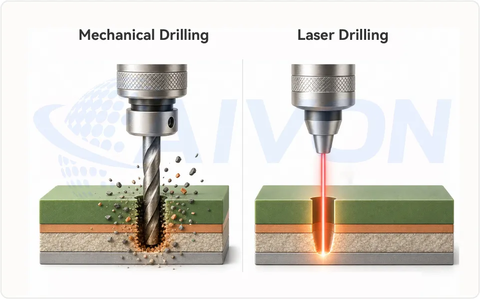
    5.  Drilling and Via Formation: Laser or mechanical drilling followed by desmear and copper plating for multilayer interconnects.

    6.  Coverlay Lamination and Patterning: Precise alignment and windowing for component pads.

    7.  Surface Finish Application: Selective plating or immersion processes.

    8.  Stiffener Attachment, Singulation, and Testing: Precision punching or routing, electrical testing, and AOI inspection.

    Quality Control in FPC Manufacturing:

    Quality consistency in flexible PCB production depends on tightly controlled process parameters across lamination, imaging, etching, and plating stages. Each CTQ directly impacts dimensional stability, electrical performance, and long-term reliability.

    ● Lamination temperature uniformity: Ensures stable resin flow and prevents interlayer stress variation, which directly affects warpage and delamination risk.

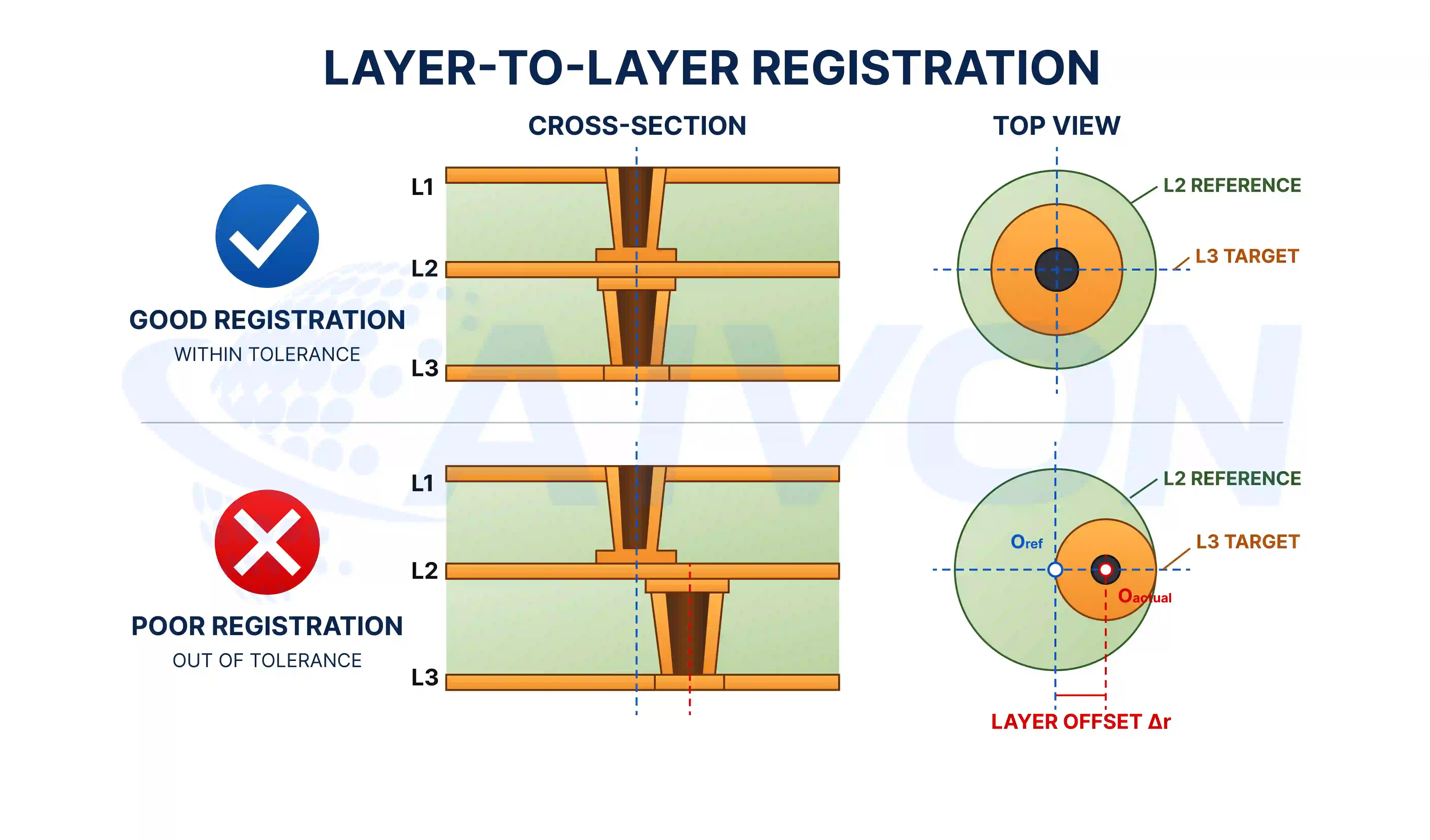
    ● Registration accuracy: Critical for multilayer alignment and fine-line circuitry; misregistration can lead to impedance variation and circuit open/short defects.

    ● Etch rate control to prevent undercutting: Maintains consistent conductor geometry and minimizes lateral undercut, which is essential for impedance control and fine pitch definition.

    ● Plating thickness uniformity: Directly influences current carrying capability and long-term fatigue resistance, especially in dynamic flex regions.

    ● Cleanliness levels: Reduces particulate contamination that can cause voids, adhesion failure, or micro-short defects in high-density circuits.

    Compliance with IPC-6013, IATF 16949 (automotive), and ISO 13485 (medical) requires extensive documentation, statistical process control, and regular capability studies.

    Common Flexible PCB Manufacturing Defects and Their Causes

    FPC manufacturing defects can significantly impact product reliability, yield, and overall production efficiency in flexible circuit fabrication. Understanding the most common FPC failure modes, along with their root causes and prevention strategies, is essential for improving process control and manufacturing quality.

    1. Dynamic Fatigue Cracking

    Root causes: Tight bend radii, repeated flexing cycles, excessive copper thinning(FPC Copper Thinning, Trace Width and Etching Control) during fabrication, uneven copper distribution, or material defects introduced during manufacturing.

    Prevention: Use high-ductility RA copper, maintain consistent copper thickness throughout the etching process, optimize plating uniformity, and implement rigorous process controls to minimize stress concentration points.

    Manufacturing Consideration: Even when the flex circuit design is mechanically sound, excessive copper reduction caused by over-etching or poor process control can significantly shorten flex life. Variations in trace geometry, copper thickness retention, and etching uniformity may create localized weak points that accelerate crack initiation under repeated bending.

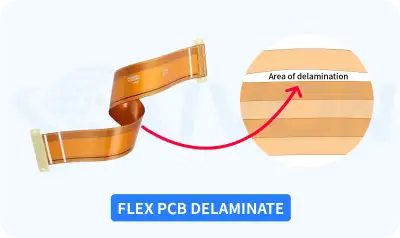
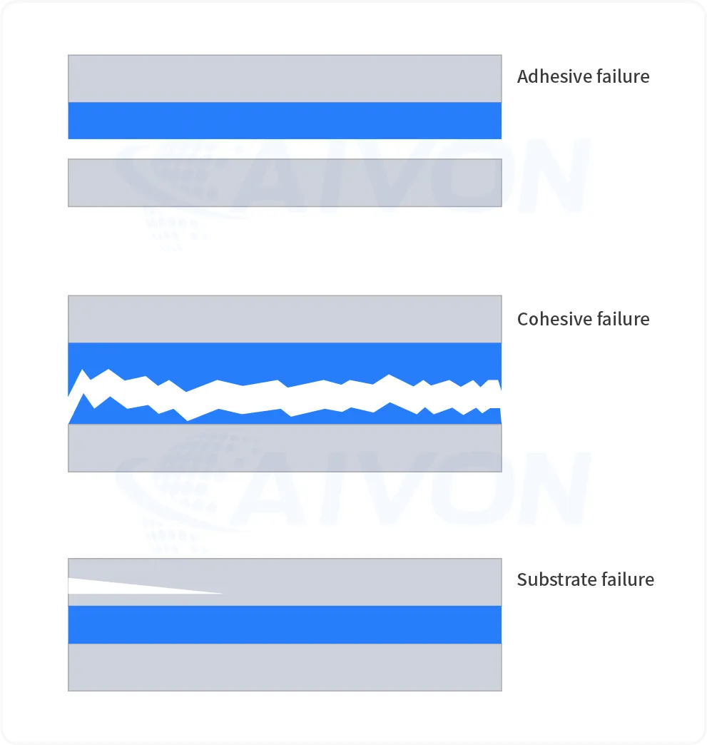
    2.  Delamination

    FPC Delamination

    Root causes: Moisture entrapment, inadequate surface preparation, contamination, thermal mismatch between materials, or insufficient lamination pressure.

    Prevention: Pre-bake incoming materials, optimize vacuum lamination profiles, implement plasma surface treatment, and conduct routine peel strength verification.

    Manufacturing Consideration: Delamination is often linked to inconsistencies in lamination processing rather than material selection alone. Factors such as moisture content, pressure distribution, temperature ramp rates, and adhesive flow behavior directly influence bond integrity and long-term reliability.

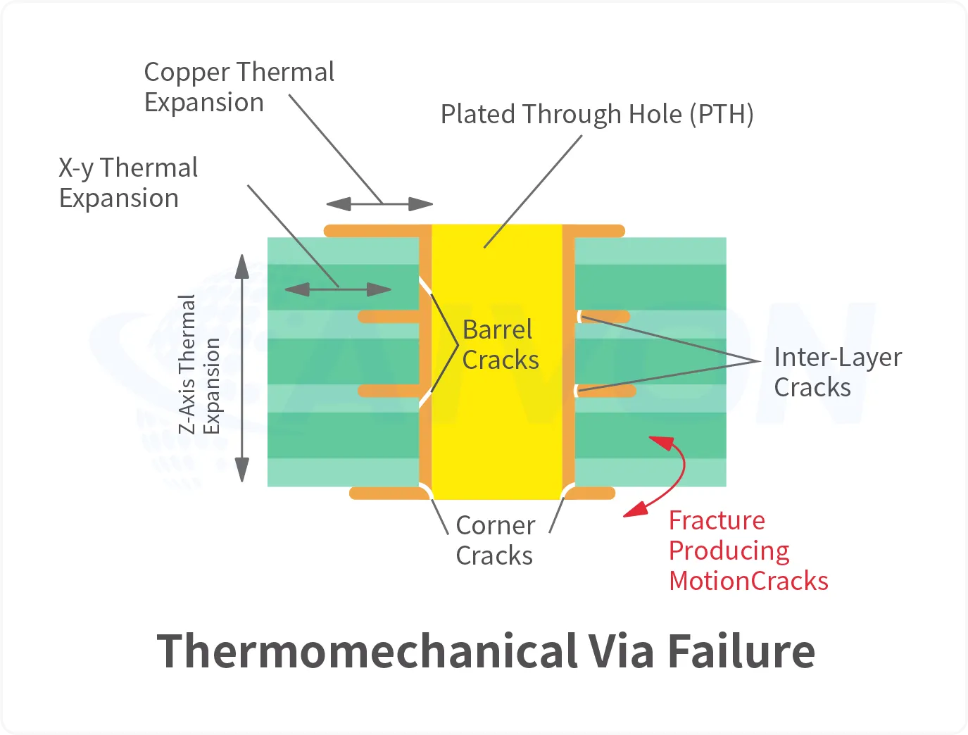
    3.  Copper Cracking at Plated Through Holes (PTH)

    Copper Cracking at Plated Through Holes

    Root causes: Brittle copper deposits, insufficient plating thickness, thermal cycling stress, or defects introduced during drilling and metallization.

    Prevention: Optimize copper plating chemistry, maintain uniform plating thickness, improve hole wall preparation, and verify plating quality through cross-section analysis.

    Manufacturing Consideration: PTH reliability depends heavily on drilling quality, desmear effectiveness, and copper plating consistency. Variations in hole wall preparation or plating ductility can create stress concentration zones that eventually lead to barrel cracking and electrical failure.

    4.  Coverlay Voids and Adhesion Failure

     Coverlay Voids

    Root causes: Surface contamination, trapped air, improper vacuum lamination settings, adhesive flow issues, or material incompatibility.

    Prevention: Implement strict cleaning procedures, optimize lamination pressure and temperature profiles, utilize vacuum-assisted lamination, and perform routine cross-section inspections.

    Manufacturing Consideration: Coverlay quality is highly sensitive to lamination conditions. Poor vacuum performance, inadequate adhesive flow, or inaccurate alignment can result in void formation, lifting, and reduced environmental protection of the circuitry.

    CEZON Case Study: Coverlay Delamination on Thick Copper FPC

    Customer Requirement:

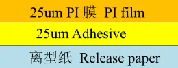
    A customer required a 2-layer flexible PCB with a finished copper thickness of 80 μm. The initial design used our standard coverlay construction, model ASC-FC125SKT1, which consists of 25 μm polyimide film with a 25 μm adhesive layer.

    Challenge:

    After lamination and subsequent processing, localized delamination occurred between the coverlay and the copper surface. In some areas, the coverlay even cracked during handling and assembly. This significantly weakened the mechanical integrity of the flex circuit and posed a reliability risk.

    Root Cause Analysis:

    The root cause was insufficient adhesive thickness relative to the copper profile. With an 80 μm finished copper thickness, the 25 μm adhesive layer lacked adequate volume and flow capability to properly encapsulate the copper traces and fill the spaces between them. This resulted in reduced bonding area and weak interfacial adhesion. Once delamination initiated, the coverlay lost mechanical support and became prone to cracking under even moderate handling stress.

    In practice, we have observed that when finished copper thickness exceeds approximately 50–60 μm, standard 25 μm adhesive coverlay often becomes marginal, especially in designs with dense traces or larger copper features.

    Solution:

    The coverlay construction was changed from 25 μm PI + 25 μm adhesive to 25 μm PI + 50 μm adhesive. The thicker adhesive provided significantly better resin flow and encapsulation around the thick copper, greatly increasing the effective bonding area and interfacial strength between the coverlay and copper surface.

    Result:

    After implementing the revised coverlay, the delamination issue was completely resolved. The flex circuits passed subsequent mechanical handling, bending, and reliability verification with no further coverlay-related defects. The change also improved overall structural robustness without compromising flexibility in non-critical areas.

    Engineering Note:

    This case highlights an important DFM consideration: adhesive thickness in coverlay selection should be evaluated based on finished copper thickness, not just nominal design requirements. For designs with finished copper ≥ 70 μm, we generally recommend evaluating 50 μm adhesive coverlay early in the design stage to avoid adhesion and mechanical strength issues during production and assembly.

    Flexible PCB Manufacturing for Different Industries

    Flexible PCB for Automotive Electronics

    Automotive electronics use flexible circuits in displays, lighting, sensors, battery systems, cameras, and control modules.

    Designs in the flexible PCB for automotive should consider temperature changes, vibration, mechanical movement, electrical requirements, and long-term reliability. Material selection and bend-area design are especially important for circuits installed in moving or confined spaces.

    Flexible Circuits for Medical Devices

    Medical devices often require compact, lightweight, and reliable interconnections.

    FPCs may be used in diagnostic equipment, monitoring devices, imaging systems, and wearable medical products. The design should consider cleanliness, insulation, flexibility, biocompatibility requirements where applicable, and the conditions of use.

    Flexible PCBs for Wearable Devices

    Wearable products require lightweight and flexible structures. The wearable flexible PCB can help connect sensors, displays, batteries, and other compact electronic components.

    The circuit should be designed around the product’s movement and shape. Bend radius, material thickness, component placement, and protective layers all affect comfort and reliability.

    Flexible Circuits for Aerospace and Defense Systems

    Aerospace flexible PCB solutions are used in applications where compact routing, weight control, vibration resistance, and stable electrical performance are important. Flexible circuits can help connect components in confined spaces while supporting lightweight and complex system designs.

    Material selection and manufacturing controls should be matched to the operating environment. Depending on the application, the aerospace flexible PCB may also require application-specific inspection, environmental testing, and reliability validation.

    Flexible PCBs for Consumer Electronics

    Consumer electronics commonly use FPCs in phones, tablets, cameras, displays, keyboards, and other compact devices.

    These applications often require a balance between thinness, flexibility, fine features, assembly compatibility, and cost.

    Flexible Circuits for Industrial and Telecommunications Equipment

    Industrial and telecommunications equipment may use flexible circuits for displays, sensors, control panels, connectors, and compact internal wiring.

    The material and circuit structure should be selected according to the electrical load, mechanical conditions, temperature, and expected service life.

    Rigid-Flex vs Pure Flex Decision Framework:

    ● Pure Flex: Maximum conformability and lowest weight.

    ● Rigid-Flex: Better component stability and assembly yields.

    ● Total cost analysis often favors rigid-flex in complex systems despite higher upfront tooling.

    Engineers should conduct thorough design reviews, prototype validation, and supply chain qualification early in the development cycle.

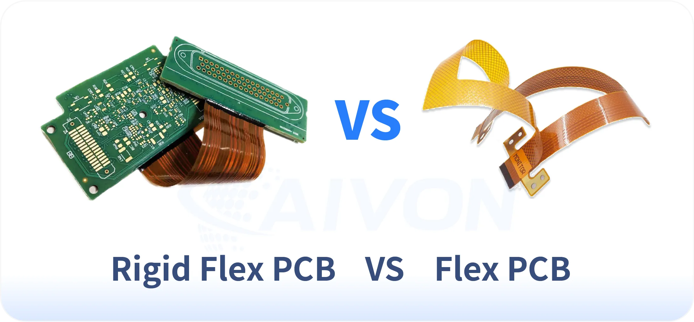
    FPC vs Rigid-Flex: Manufacturing and Material Selection Trade-offs

    Comparison of pure FPC and rigid-flex PCB structures

    From a production and material selection perspective, choosing between pure Flexible PCB (FPC) and Rigid-Flex constructions involves balancing manufacturing complexity, material cost, process yield, and production scalability.

    Pure FPC uses flexible substrates (primarily PI or PET) throughout the entire circuit. Manufacturing is specialized but relatively streamlined, focusing on flexible material handling, precise coverlay alignment, and singulation. Production advantages include lower material diversity, simpler lamination cycles in many cases, and better suitability for high-volume dynamic flex applications. However, attaching components can be more challenging, often requiring additional stiffeners, which adds secondary bonding processes.

    Rigid-Flex combines rigid PCB areas (typically FR-4 or high-Tg materials) with flexible PI sections in a single laminated structure. This hybrid approach significantly increases manufacturing complexity. It requires multiple lamination cycles, precise zonal registration between rigid and flex materials, and careful management of CTE mismatch at transition zones. Production yields are generally lower than pure FPC, especially in multilayer builds, due to higher risk of delamination, warpage, and via stress at the rigid-flex interface.

    Key Manufacturing and Material Comparison:

     Property

    Pure FPC

    Rigid-Flex

    Material Cost

    Pure FPC is usually lower cost as it uses uniform flexible materials.

    Rigid-Flex requires both rigid laminates and flexible PI films, plus specialized no-flow prepregs, increasing material cost by 40-80%.

    Process Complexity

    Pure FPC involves fewer lamination steps.

    Rigid-Flex requires sequential lamination (often 3-5 stages), plasma desmear optimization for different material types, and more stringent registration control (±25μm or tighter).

    Production Yield

    Pure FPC typically achieves higher yields (85-95% in mature processes)

    Rigid-Flex yields are lower (70-85%) due to interface challenges, especially in high-layer counts.

    Lead Time

    Pure FPC prototypes and production are faster.

    Rigid-Flex often adds 1-2 weeks due to complex tooling and multi-stage lamination.

    Scalability

    Pure FPC is easier to scale for high-volume consumer applications.

    Rigid-Flex is better suited for medium-volume, high-reliability programs (automotive, medical, aerospace).

    Conclusion

    Successful flexible PCB manufacturing depends on the right combination of materials, circuit structure, fabrication processes, and quality controls.

    Polyimide, copper foil, coverlay, adhesives, stiffeners, and surface finishes all influence the performance of the finished FPC. At the same time, trace routing, bend radius, layer registration, lamination, plating, and inspection must be carefully managed during flex PCB fabrication.

    Whether the project requires a simple single-sided circuit, a multilayer FPC, a dynamic-flex design, or a rigid-flex structure, early design review and close communication with the manufacturer can help reduce production risks.

    By selecting materials based on actual application requirements and validating the manufacturing process before volume production, engineers can achieve more reliable, manufacturable, and cost-effective flexible circuit solutions.

    FAQs

    Q1: When is RA copper preferred over ED copper?

    A1: RA copper is preferred for applications requiring frequent bending or long flex life because of its excellent fatigue resistance. ED copper is generally suitable for static flex designs where cost efficiency is a higher priority.

    Q2: How many bend cycles can a quality PI FPC achieve?

    A2: A well-designed PI-based FPC can typically withstand more than 500,000 bend cycles, with some dynamic flex applications achieving several million cycles. Actual performance depends on factors such as bend radius, copper type, and circuit design.

    Q3: What standards apply to automotive and medical FPC production?

    A3: Automotive FPCs are commonly manufactured under IATF 16949 quality systems and IPC-6013 requirements. Medical FPCs typically follow ISO 13485 standards and require enhanced traceability and process control.

    Q4: How does coverlay thickness impact performance?

    A4: Thicker coverlays provide better mechanical protection and insulation but reduce overall flexibility. Most FPC designs use coverlays between 25 μm and 50 μm to balance durability and bending performance.

    Q5: What are typical lead times for custom FPC projects?

    A5: Prototype FPC projects typically require 8 to 20 days, while production volumes often take 2 to 5 weeks depending on design complexity and material availability. Early design validation can help shorten development timelines.

    Q6: How do material choices affect total project cost?

    A6: Material selection influences not only manufacturing cost but also reliability, yield, and product lifespan. Higher-performance materials often reduce long-term failure risks and can lower the overall cost of ownership.

    Q7: Are there cost-effective alternatives to FPCs for large EV battery packs?

    A7: For large EV battery packs, busbars, wire harnesses, flexible flat cables (FFCs), and modular wiring assemblies may be cost-effective alternatives to FPCs. Busbars are suitable for high-current connections, while wire harnesses and FFCs can support battery monitoring and signal routing. The best option depends on the pack structure, electrical requirements, available space, and assembly process.

    Q8: What factors should be considered when selecting FPC materials?

    A8: FPC material selection should consider flexibility, bend requirements, operating temperature, electrical performance, mechanical strength, and environmental exposure. The material should match the circuit structure and the conditions expected during assembly and use.

    Q9: How can designers reduce the cost of flexible PCB manufacturing?

    A9: Designers can help control flexible PCB manufacturing costs by simplifying the circuit structure, avoiding unnecessary tight tolerances, selecting practical material options, and improving panel utilization. Early DFM review can also reduce redesigns and production issues.

    Q10: What is the difference between FPC fabrication and FPC assembly?

    A10: FPC fabrication produces the flexible circuit itself, including its conductive pattern, insulation, openings, and surface finish. FPC assembly adds components, connectors, or other parts to the fabricated circuit. Some applications require only bare FPCs, while others need a complete flexible circuit assembly.

    Q11: How can flexible circuits be protected during installation and operation?

    A11: Flexible circuits can be protected through suitable reinforcement, connector support, controlled routing, and secure fixing. Designers should avoid sharp bends, excessive mechanical stress, and unsupported areas that may be damaged during installation or repeated movement.

    Q12: What should be considered when choosing an FPC manufacturer?

    A12: When choosing an FPC manufacturer, consider its material capabilities, fabrication experience, DFM support, inspection methods, prototype services, production capacity, and quality documentation. The supplier should also be able to meet the reliability and traceability requirements of the intended application.

    Get in Touch


      Specifications
      Category Capability Details
      PCB Material Brand Goldenmax GL11,Guangzhou Aluminum (Goldenmax GL11,Guangzhou Aluminum)
      SolderMask LB Brand LB-1900W
      Copper Thickness 18um/25um/35um/70um(0.5oz/0.75oz/1oz/2oz) Refers to the thickness of finished PCB outer copper,0.5oz=18um,1oz=35um
      PCB Thickness 0.8-2.0mm 0.8/1.0/1.2/1.6/2.0 mm
      Thickness Tolerance( thickness≥1.0mm) ≤10 Thickness measurement position is the thickest position of the whole PCB (including copper + Soldermask + Silkscreen)
      PCB Thickness Tolerance (Thickness <1.0mm) ±0.1mm Thickness measurement position is the thickest position of the whole PCB (including copper + Soldermask + Silkscreen)
      Minimum Trace Width ≤10 At present,we can process min 8mil trace width,and ≥10mil is advised
      Minimum Trace Distance 8mil(0.2mm) At present,we can process min 8mil trace distance,and ≥10mil is advised
      Drilling Aperture Hole size≥ PCB thickness ≥1.0mm The minimum hole shall not be less than the thickness of the PCB, and it shall not be less than 1.0mm
      Drilling Hole Tolerance ±0.1mm Hole tolerance is ±0.1mm, for example, designed for 1.5mm hole, the drilling hole of the final PCB in 1.4-1.6mm is normal.
      Soldermask Type Photosensitive ink Photosensitive ink is now the most used type, thermosetting oil is generally used in low-grade light panels
      Soldermask Bridge 0.15mm If the soldmask color is green or blue, the pad spacing must be bigger than or equal to 8mil; White and black ink pad spacing ≥10mil
      Minimum Silkscreen Width ≥0.15mm Minimum width of characters is 0.15mm, if less than 0.15mm, the physical board may cause unclear characters due to design reasons.
      Minimum Silkscreen Height ≥1.0mm Minimum height of characters is 0.8mm. If the height is less than 0.8mm, the characters may be unclear due to design reasons
      Max Size Standard:480x580mm
      Max:580x1180mm
      The limit size is the maximum size that can be machined, but the cost will increase due to plate waste and high processing costs
      Dimension Accuracy ±0.15mm CNC contour tolerance is ±0.15mm, V-Cut contour tolerance is ±0.15mm, mold shaping contour tolerance is ±0.1mm
      Panel: no gap between the panel 0mm The gap between the PCBs is 0mm
      Panel: there are gaps between the panel 2.0mm If you want space between each PCB while panelling, the distance should be bigger than 2.0mm.

      Get in Touch


        PCB Assembly Capabilities Overview
        Category Details
        Lead Time 1. Regular prototyping orders can be finished in 1-2 days 2. Small batches take 3 days (expedited service available in 24 hours) 3. Medium batches will take 5 days or more, scheduled delivery is recommended for long-term demands Remark: Lead time will be calculated after PCB, components, and necessary documents are ready (BOM, CAD, Gerber file, and other design drawings, etc.)
        PCBA SMT+DIP Equipments 1. Seven Siemens high-speed and high-accuracy SMT production lines 2. Three DIP production lines (automatic wave-soldering)+ 2 manual soldering lines 3. Three Assembly and testing lines
        PCBA Capacity SMT Capacity: 10 million points per day DIP Capacity: 180,000 points per day 30-50 different designs per day (single shift)
        Components Service Turnkey AIVON has established a complete and reliable supplier network, which enables us to get qualified components at reasonable prices
        Kitted or Consigned Customers provide all components, and we do the assembly work To ensure the PCBA quality, all components shall be packaged in tube, tape, tray or reel to suit our assembly machine
        Partial Turnkey Customers provide the major components and we buy the rest
        PCBA Solder Type SMT, THT, single or double side PnP
        Solder Paste/Tin Wire/Tin Bar Both lead and lead-free (RoHS compliant) are available
        Stencil High-accuracy laser cutting stencil to ensure good printing performance such as Fine-pitch ICs and BGA to meet IPC-2 Class or higher
        MOQ no MOQ required for customers with R&D purposes
        Component Size Minimum Package 01005 chip size
        Minimum BGA Spacing 0.3mm(ball to ball)
        Minimum Fine Pitch 0.25mm (X-ray available to ensure the solder quality)
        Component Package We accept tape and reel, tube, and tray packages for components
        Maximum Mount Accuracy of Components (100FP) ±50 μm
        Solderable PCB Type Rigid PCB, FPC, Rigid-Flex PCB, Aluminum PCB
        PCB Size Min PCB size:50mm x 50mm (boards under this size will be panelized) Max PCB size:350mm x 1200mm
        Testing and coverage We will apply a variety of testing to the PCBA in mount or already mount to ensure the quality before shipping
        IQC: incoming inspection Reject the defective material to avoid loss in the production line
        SPI: solder paste inspection 1. Real-time monitoring of Height/Area/Volume of solder paste 2. Capture the defect of the solder bridge, insufficient or excessive solder, and poor shape of the solder
        Online AOI inspection 1. Inspect the soldering performance of all parts, also include the polarity of components 2. 3D AOI can catch the defect of tiny lift of QFP pins
        SMT sample inspection FAI check refers to the BOM and Gerber data, to make sure all the components are correctly mounted, and prevent defects from getting into the next process
        IPQC inspection In-process inspection and verification of SMT&DIP production system, double check for each process
        Offline AOI inspection Inspect for defects such as wrong parts, parts missing, and wrong polarity
        X-Ray inspection Inspect the solder joint of BGA, QFN, and other high-precision components which are invisible to human-eye
        Functional Testing 1. The customer provides the test program and test method, we can follow up 2. Highly recommend customers conduct functional tests (especially for massive products) before shipping to prevent any defects
        Repair & Rework We offer repair services for any soldering defects

        Get in Touch


          Specifications
          Category Small and Medium Batches Order (Order area ≥10㎡) Prototype Order (Order area < 3㎡)
          Product structure 1+n+1; 1+1+n+1+1; 2+n+2 1+n+1; 1+1+n+1+1; 2+n+2
          F+R, cu+F+cu, R+F+R+F+R, R+F+R F+R, cu+F+cu, R+F+R+F+R, R+F+R
          Number of layers Rigid-flex PCB ≤18L ≤24L
          FPC ≤10L ≤16L
          Board thickness (mm) Rigid-flex board 0.3-3.2 0.3-3.2
          FPC 0.06-0.35 0.06-0.35
          Board size (mm) Rigid-flex PCB 15*15 to 310*510 15*15 to 310*510
          FPC 5*15 to 310*510 5*15 to 310*510
          Copper thickness (OZ) Maximum copper thickness of FR-4 Outer layer 2OZ, inner layer 2OZ Outer layer 2OZ, inner layer 2OZ
          Maximum copper thickness of FPC Outer layer 1 OZ, inner layer 1 OZ Outer layer 2 OZ, inner layer 2 OZ
          Minimum copper trace width and spacing capability (um) 75/75 75/75
          Minimum diameter of mechanical drill (mm) 0.2 0.15
          Rigid part material Tg170 S1000-2M,IT180A S1000-2M,IT180A
          High TG halogen-free S1165 S1165
          Thickness of dielectric layer (mm) 0.1-3.2 0.075-3.2
          Flex part material Flexible material PI DuPont, Panasonic, Shengyi PI DuPont, Panasonic, Shengyi
          Surface insulation layer Cover film, soldermask Cover film, soldermask
          Thickness of dielectric layer (mm) 0.025-0.1 0.012-0.1
          Surface treatment Rigid-flex board HASL with lead / lead-free, immersion gold, immersion tin, immersion silver, OSP, HASL + gold finger, immersion gold + gold finger, nickel palladium gold, OSP + gold finger , immersion gold + OSP HASL with lead / lead-free, immersion gold, immersion tin, immersion silver, OSP, HASL + gold finger, immersion gold + gold finger, nickel palladium gold, OSP + gold finger , immersion gold + OSP
          FPC FPC HASL with lead / lead-free, immersion gold, OSP
          Stack Up
          4 conductive layers RFPC
          • 1.0mm
          • 1.6mm

          Rigid part

          Flex part


          top soldermask layer

          20um


          rigid-top copper layer

          Copper

          18um(Finished Copper thickness 35um)


          FR4

          400um

          PI

          12.5um


          Pure gum

          13um

          Adhesive

          15um

          flex-copper 2 layer

          Copper

          18um

          Copper

          18um


          Adhesive

          20um

          Adhesive

          20um


          PI

          25um

          PI

          25um


          Adhesive

          20um

          Adhesive

          20um

          flex-copper 3 layer

          Copper

          18um

          Copper

          18um


          Pure gum

          13um

          Adhesive

          15um


          FR4

          400um

          PI

          12.5um

          rigid-bottom copper layer

          Copper

          18um(Finished Copper thickness 35um)


          bottom soldermask layer

          20um


          Total thickness

          1003um

          FPC Thickness

          156um

          Rigid part

          Flex part


          top soldermask layer

          20um


          rigid-top copper layer

          Copper

          18um(Finished Copper thickness 35um)


          FR4

          700um

          PI

          12.5um


          Pure gum

          13um

          Adhesive

          15um

          flex-copper 2 layer

          Copper

          18um

          Copper

          18um


          Adhesive

          13um

          Adhesive

          13um


          PI

          25um

          PI

          25um


          Adhesive

          13um

          Adhesive

          13um

          flex-copper 3 layer

          Copper

          18um

          Copper

          18um


          Pure gum

          13um

          Adhesive

          15um


          FR4

          700um

          PI

          12.5um

          rigid-bottom copper layer

          Copper

          18um(Finished Copper thickness 35um)


          bottom soldermask layer

          20um


          Total thickness

          1589um

          FPC Thickness

          142um

          Get in Touch


            Specifications
            Category Capability Details
            Board Size Min(pcs) 1*0.5mm
            Max (Pnl Size) 250*1200mm
            Base Material Thickness 0.06——0.3mm
            Board Thickness 0.1-0.5mm
            Base Copper Thickness 1/3OZ——2OZ
            PTH Hole Wall Copper Thickness 8-20μm
            Blind Hole Filling Capacity Aspect Ratio (Hole Size: Hole Depth) 01:10:00
            Blind Hole Filling Capacity (Hole Size) 50-150μm
            Single Line Impedance Tolerance ≤10
            Differential Impedance Tolerance ≤10
            Min Track/Spacing (Double Layers Board) Surface Copper Thickness:8-14μm 40/40 um
            Surface Copper Thickness:15-20μm 45/45 um
            Surface Copper Thickness:21-30μm 55/55 um
            Surface Copper Thickness:31-40μm 75/75 um
            Surface Copper Thickness:≥40μm 80/80 um
            Line Width Tolerance Line Width≤0.050mm ±.02mm
            0.05mm<Line Width≤0.15mm ±20°
            Line Width>0.150mm ≤10
            Silkscreen Silkscreen Character Min Width/Spacing 4mil
            Cell_SolderMask Green Solder Mask Thickness Range 10~30 μm
            Related Capacity Dimension Tolerance from Line Edge to Plate Edge ±0.25 mm
            Stack Up
            1 conductive layer FPC
            • 0.08mm
            • 0.1mm
            • 0.13mm
            • 0.15mm

            top coverlay

            PI

            12.5um

            Adhesive

            15um

            top copper layer

            Copper

            18um(Finished Copper thickness 18um)


            Adhesive

            13um


            PI

            25um

            Total thickness


            83.5um

            top coverlay

            PI

            25um

            Adhesive

            25um

            top copper layer

            Copper

            18um(Finished Copper thickness 18um)


            Adhesive

            13um


            PI

            25um

            Total thickness


            106um

            top coverlay

            PI

            25um

            Adhesive

            25um

            top copper layer

            Copper

            35um(Finished Copper thickness 35um)


            Adhesive

            20um


            PI

            25um

            Total thickness


            130um

            top coverlay

            PI

            25um

            Adhesive

            25um

            top copper layer

            Copper

            70um(Finished Copper thickness 70um)


            Adhesive

            0um


            PI

            25um

            Total thickness


            145um

            2 conductive layers FPC
            • 0.1mm
            • 0.13mm
            • 0.15mm
            • 0.18mm
            • 0.2mm
            • 0.23mm
            • 0.26mm

            top coverlay

            PI

            12.5um

            Adhesive

            15um

            top copper layer

            Copper

            12um(Finished Copper thickness 18um)


            Adhesive

            0um


            PI

            25um


            Adhesive

            0um

            bottom copper layer

            Copper

            12um(Finished Copper thickness 18um)

            bottom coverlay

            Adhesive

            15um

            PI

            12.5um

            Total thickness


            104um

            top coverlay

            PI

            12.5um

            Adhesive

            15um

            top copper layer

            Copper

            18um(Finished Copper thickness 35um)


            Adhesive

            13um


            PI

            12.5um


            Adhesive

            13um

            bottom copper layer

            Copper

            18um(Finished Copper thickness 35um)

            bottom coverlay

            Adhesive

            15um

            PI

            12.5um

            Total thickness


            129.5um

            top coverlay

            PI

            12.5um

            Adhesive

            15um

            top copper layer

            Copper

            18um(Finished Copper thickness 35um)


            Adhesive

            20um


            PI

            25um


            Adhesive

            20um

            bottom copper layer

            Copper

            18um(Finished Copper thickness 35um)

            bottom coverlay

            Adhesive

            15um

            PI

            12.5um

            Total thickness


            156um

            top coverlay

            PI

            25um

            Adhesive

            25um

            top copper layer

            Copper

            18um(Finished Copper thickness 35um)


            Adhesive

            13um


            PI

            25um


            Adhesive

            13um

            bottom copper layer

            Copper

            18um(Finished Copper thickness 35um)

            bottom coverlay

            Adhesive

            25um

            PI

            25um

            Total thickness


            187um

            top coverlay

            PI

            25um

            Adhesive

            25um

            top copper layer

            Copper

            18um(Finished Copper thickness 35um)


            Adhesive

            20um


            PI

            25um


            Adhesive

            20um

            bottom copper layer

            Copper

            18um(Finished Copper thickness 35um)

            bottom coverlay

            Adhesive

            25um

            PI

            25um

            Total thickness


            201um

            top coverlay

            PI

            25um

            Adhesive

            25um

            top copper layer

            Copper

            35um(Finished Copper thickness 50um)


            Adhesive

            20um


            PI

            25um


            Adhesive

            20um

            bottom copper layer

            Copper

            35um(Finished Copper thickness 50um)

            bottom coverlay

            Adhesive

            25um

            PI

            25um

            Total thickness


            235um

            top coverlay

            PI

            25um

            Adhesive

            25um

            top copper layer

            Copper

            70um(Finished Copper thickness 70um)


            Adhesive

            0um


            PI

            25um


            Adhesive

            0um

            bottom copper layer

            Copper

            70um(Finished Copper thickness 70um)

            bottom coverlay

            Adhesive

            25um

            PI

            25um

            Total thickness


            265um

            4 conductive layers FPC
            • 0.2mm
            • 0.23mm
            • 0.26mm
            • 0.3mm
            • 0.35mm

            top coverlay

            PI

            12.5um

            Adhesive

            15um

            top copper layer

            Copper

            12um(Finished Copper thickness 18um)


            Adhesive

            0um


            PI

            25um


            Pure gum

            13um

            copper 2 layer

            Copper

            12um


            Adhesive

            0um


            PI

            25um


            Adhesive

            0um

            copper 3 layer

            Copper

            12um


            Pure gum

            13um


            PI

            25um


            Adhesive

            0um

            bottom copper layer

            Copper

            12um(Finished Copper thickness 18um)

            bottom coverlay

            Adhesive

            15um

            PI

            12.5um

            Total thickness


            204um

            top coverlay

            PI

            12.5um

            Adhesive

            15um

            top copper layer

            Copper

            12um(Finished Copper thickness 18um)


            Adhesive

            0um


            PI

            25um


            Pure gum

            13um

            copper 2 layer

            Copper

            18um


            Adhesive

            13um


            PI

            12.5um


            Adhesive

            13um

            copper 3 layer

            Copper

            18um


            Pure gum

            13um


            PI

            25um


            Adhesive

            0um

            bottom copper layer

            Copper

            12um(Finished Copper thickness 18um)

            bottom coverlay

            Adhesive

            15um

            PI

            12.5um

            Total thickness


            229.5um

            top coverlay

            PI

            12.5um

            Adhesive

            15um

            top copper layer

            Copper

            18um(Finished Copper thickness 35um)


            Adhesive

            13um


            PI

            25um


            Pure gum

            13um

            copper 2 layer

            Copper

            18um


            Adhesive

            13um


            PI

            12.5um


            Adhesive

            13um

            copper 3 layer

            Copper

            18um


            Pure gum

            13um


            PI

            25um


            Adhesive

            13um

            bottom copper layer

            Copper

            18um(Finished Copper thickness 35um)

            bottom coverlay

            Adhesive

            15um

            PI

            12.5um

            Total thickness


            267.5um

            top coverlay

            PI

            25um

            Adhesive

            25um

            top copper layer

            Copper

            18um(Finished Copper thickness 35um)


            Adhesive

            13um


            PI

            25um


            Pure gum

            13um

            copper 2 layer

            Copper

            18um


            Adhesive

            0um


            PI

            25um


            Adhesive

            0um

            copper 3 layer

            Copper

            18um


            Pure gum

            13um


            PI

            25um


            Adhesive

            13um

            bottom copper layer

            Copper

            18um(Finished Copper thickness 35um)

            bottom coverlay

            Adhesive

            25um

            PI

            25um

            Total thickness


            299um

            top coverlay

            PI

            25um

            Adhesive

            25um

            top copper layer

            Copper

            18um(Finished Copper thickness 35um)


            Adhesive

            13um


            PI

            25um


            Pure gum

            25um

            copper 2 layer

            Copper

            18um


            Adhesive

            13um


            PI

            25um


            Adhesive

            13um

            copper 3 layer

            Copper

            18um


            Pure gum

            25um


            PI

            25um


            Adhesive

            13um

            bottom copper layer

            Copper

            18um(Finished Copper thickness 35um)

            bottom coverlay

            Adhesive

            25um

            PI

            25um

            Total thickness


            349um

            6 conductive layers FPC
            • 0.3mm
            • 0.37mm

            top coverlay

            PI

            12.5um

            Adhesive

            15um

            top copper layer

            Copper

            12um(Finished Copper thickness 18um)


            Adhesive

            0um


            PI

            25um


            Pure gum

            13um

            copper 2 layer

            Copper

            12um


            Adhesive

            0um


            PI

            25um


            Adhesive

            0um

            copper 3 layer

            Copper

            12um


            Pure gum

            13um


            Coverlay

            27.5um

            copper 4 layer

            Copper

            12um


            Adhesive

            0um


            PI

            25um


            Adhesive

            0um

            copper 5 layer

            Copper

            12um


            Pure gum

            13um


            PI

            25um


            Adhesive

            0um

            bottom copper layer

            Copper

            12um(Finished Copper thickness 18um)

            bottom coverlay

            Adhesive

            15um

            PI

            12.5um

            Total thickness


            293.5um

            top coverlay

            PI

            12.5um

            Adhesive

            15um

            top copper layer

            Cooper

            12um(Finished cooper thickness 18um)


            Adhesive

            13um


            PI

            25um


            Pure gum

            13um

            copper 2 layer

            Cooper

            12um


            Adhesive

            13um


            PI

            25um


            Adhesive

            13um

            copper 3 layer

            Cooper

            12um


            Pure gum

            13um


            Coverlay

            27.5um

            copper 4 layer

            Cooper

            12um


            Adhesive

            13um


            PI

            25um


            Adhesive

            13um

            copper 5 layer

            Cooper

            12um


            Pure gum

            13um


            PI

            25um


            Adhesive

            13um

            bottom copper layer

            Cooper

            12um(Finished cooper thickness 18um)

            bottom coverlay

            Adhesive

            15um

            PI

            12.5um

            Total thickness


            371.5um

            8 conductive layers FPC
            • 0.38mm
            • 0.48mm

            top coverlay

            PI

            12.5um

            Adhesive

            15um

            top copper layer

            Copper

            12um(Finished Copper thickness 18um)


            Adhesive

            0um


            PI

            25um


            Pure gum

            13um

            copper 2 layer

            Copper

            12um


            Adhesive

            0um


            PI

            25um


            Adhesive

            0um

            copper 3 layer

            Copper

            12um


            Pure gum

            13um


            Coverlay

            27.5um

            copper 4 layer

            Copper

            12um


            Adhesive

            0um


            PI

            25um


            Adhesive

            0um

            copper 5 layer

            Copper

            12um


            Pure gum

            13um


            Coverlay

            27.5um

            copper 6 layer

            Copper

            12um


            Adhesive

            0um


            PI

            25um


            Adhesive

            0um

            copper 7 layer

            Copper

            12um


            Pure gum

            13um


            PI

            25um


            Adhesive

            0um

            bottom copper layer

            Copper

            12um(Finished Copper thickness 18um)

            bottom coverlay

            Adhesive

            15um

            PI

            12.5um

            Total thickness


            383um

            top coverlay

            PI

            12.5um

            Adhesive

            15um

            top copper layer

            Cooper

            12um(Finished cooper thickness 18um)


            Adhesive

            13um


            PI

            25um


            Pure gum

            13um

            copper 2 layer

            Cooper

            12um


            Adhesive

            13um


            PI

            25um


            Adhesive

            13um

            copper 3 layer

            Cooper

            12um


            Pure gum

            13um


            Coverlay

            27.5um

            copper 4 layer

            Cooper

            12um


            Adhesive

            13um


            PI

            25um


            Adhesive

            13um

            copper 5 layer

            Cooper

            12um


            Pure gum

            13um


            Coverlay

            27.5um

            copper 6 layer

            Cooper

            12um


            Adhesive

            13um


            PI

            25um


            Adhesive

            13um

            copper 7 layer

            Cooper

            12um


            Pure gum

            13um


            PI

            25um


            Adhesive

            13um

            bottom copper layer

            Cooper

            12um(Finished cooper thickness 18um)

            bottom coverlay

            Adhesive

            15um

            PI

            12.5um

            Total thickness


            487um

            Drilling & Hole
            Category Capability Details
            Width Tolerance of White Line Smooth Place ±0.10 mm
            Bump Place ±0.20 mm
            Min Drilling Hole Size Machine Dril 0.100 mm
            Min Punching Hole Size N/A 0.50 mm
            Complete Hole Size Tolerances PTH ±0.050 mm
            NPTH ±0.025 mm
            Surface Treatment
            Category Capability Details
            Nickel Gold Plating Nickel Thickness 40~ 314U"
            Nickel Th ±78U"
            Gold Thickness 1.18U" ~ 40U"
            Min Spacing (Golden Finger or Pad) 35um
            Nickel Gold Immersion Nickel Thickness 40 ~ 236 U"
            Nickel Th ±40U"
            Gold Thickness 1U" ~ 3 U"
            Min Spacing (Golden Finger or Pad) 40um
            OSP OSP Thicknes 6U"~20U"

            Get in Touch


              HDI Manufacturing Capabilities
              Item Category Capability Parameters
              Standard Capability Sample Capability
              Product
              Type
              Any-layer Interconnect / yes yes
              HDI Structure / 3+N+3 6+N+6
              Layer Count / 16 layers 20 layers
              Surface Finish / HASL (Leaded/Lead-free), ENIG, OSP, Bare Copper, Immersion Tin, Immersion Silver, ENIG + Gold Plated Fingers, HASL + Gold Plated Fingers, ENIG + OSP
              Special Process Boards / Half-holes, Resin Plugging, Countersink Holes, Step Slots, Depth-controlled Slots, Back-drilling, Embedded Resistors, Embedded Capacitors, Embedded Copper Blocks, Metal Edge Plating, Laser-engraved QR Codes
              Base Material Material Type FR-4 (Halogenated & Halogen-free), High-frequency, High-speed Materials
              Material Suppliers Kingboard, Nan Ya, Shengyi, ITEQ, Rogers, Panasonic, Arlon, Isola
              Board Thickness Max. Production Thickness / 3.2mm 3.2mm
              Min. Production Thickness / 0.3mm 0.2mm
              Thickness Tolerance Thickness < 0.5mm ± 0.05mm ± 0.04mm
              0.5mm ≤ Thickness < 0.8mm ±10% ±10%
              0.8mm ≤ Thickness ≤ 1.0mm ± 0.08mm ± 0.08mm
              1.0mm < Thickness ≤ 1.6mm ±0.1mm ±0.1mm
              1.6mm < Thickness ≤ 2.3mm ±0.16mm ±0.13mm
              Copper Thickness Max. Inner Layer Copper / 3OZ 5OZ
              Max. Outer Layer Copper / 4OZ 6OZ
              Lamination Layer-to-layer Registration / Max. Misalignment ≤ 50um Max. Misalignment ≤ 50um
              Copper Foil Thickness / 1/3oz, 1/2oz, 1oz, 1.5oz, 2.0oz 2.5oz, 3oz
              Common PP Lamination Capability / 7628/2116/1080/106/3313/1067 1027/1017/1037 (IC Substrate Only)
              PP Dielectric Thickness Tolerance After Lamination 7628 ±10% /
              2116 ±10% /
              1080 ±10% /
              3313 ±10% /
              106 ±10% /
              1067 ±10% /
              1037 ±15% /
              1027 ±15% /
              1017 ±15% /
              Laser Drilling Hole Position Accuracy / ≤10um /
              Min. Blind Via Diameter / 70um 60um
              Drillable Hole Diameter (Surface Cu 9um, Aspect Ratio ≤ 1:1) Hole Diameter PP Type Min. Pad Size
              60um 1017/1027/1037 110um
              70um 1017/1027/1037/106/1067 120um
              80um 1017/1027/1037/106/1067 130um
              90um 1027/1037/106/1067 140um
              100um 106/1067/1078/1080 150um
              110um 106/1067/1078/1080 160um
              120um 106/1067/1078/1080/106+106 170um
              150um 1080/106+106/1080+106/1080+1080 200um
              Open-window Blind Vias (Surface Cu ≥ 13um, Aspect Ratio ≤ 1:1) 60–150um Refer to Brown-oxide Blind Vias Refer to Brown-oxide Blind Vias
              151–300um Single layer ≤ 2116; multi-layer stack each layer ≤ 1080 /
              > 300um Single layer ≤ 2116; multi-layer stack each layer ≤ 1080 /
              Mechanical Drilling Hole Diameter Min. Single Round Hole Diameter 0.15mm 0.1mm
              Max. Single Round Hole Diameter 6.5mm 6.5mm
              Min. Slot Drill Diameter 0.5mm 0.4mm
              Inner Corner Radius of Square Slot 0.4mm 0.4mm
              Hole Diameter Tolerance Single Round NPTH Hole ±50um ±38um
              Single Round PTH Hole ±76um ±50um
              Reamed Round Hole (NPTH) ±76um ±76um
              Reamed Round Hole (PTH) ±100um ±76um
              Countersink Hole Diameter (at Opening) ±152um ±127um
              Slot Width (PTH) ±76um ±50um
              Slot Width (NPTH) ±50um ±38um
              Slot Length Tolerance Long Slot (Length ≥ 2× Width) ±76um ±76um
              Short Slot (Length < 2× Width) ±4mil ±76um
              Hole Position Accuracy 1st Drill Position Accuracy ±76um ±50um
              2nd Drill Position Accuracy ±76um ±50um
              Hole Edge-to-edge Spacing Different Nets ≥254um 254um > L ≥ 200um (Use CAF-resistant Material)
              Same Net ≥200um 200um > L ≥ 152um (Note near-hole in MI, add dust-extraction re-drill)
              Slot Length Tolerance Long Slot (Length ≥ 2× Slot Width) ±76um ±76um
              Short Slot (Length < 2× Slot Width) ±100um ±76um
              Back-drilling Depth Tolerance ±100um ±76um
              Countersink Hole Angle 90º, 135º, 165º 90º, 135º, 165º
              Electroplating Horizontal Electroless Copper Production Thickness Range 0.05-3.5mm /
              Blind Via Diameter / Aspect Ratio 60-200um / 0.8:1 (Blind via count ≤ 4 million, Mini-LED) 1:1
              Min. Hole Diameter / Aspect Ratio 0.2mm hole / 8:1 10:1
              0.1mm hole / 5:1 8:1
              Via-filling VCP Production Thickness Range 0.05-3.5mm /
              Through-hole Aspect Ratio 8:1 (Hole Dia. 0.1mm) /
              Throwing Power TP ≥ 70% (Aspect Ratio ≤ 5:1) /
              TP ≥ 50% (Aspect Ratio ≤ 8:1) /
              Surface Copper Standard Deviation 4um /
              Blind Via Aspect Ratio 0.8:1 (60-200um) 1:1
              Through-hole VCP Production Thickness Range 0.3-3.5mm /
              Aspect Ratio 8:1 (Through-hole Dia. 0.1mm) /
              Throwing Power TP ≥ 80% (Aspect Ratio ≤ 6:1) /
              TP ≥ 68% (Aspect Ratio ≤ 8:1) /
              Resin Plugging Production Thickness Capability Minimum 0.3mm 0.2mm
              Maximum 3.0mm 3.2mm
              Vacuum Plugging Plugging Fullness ≥95% ≥100%
              Plugging Hole Diameter (Drill Bit) 0.15-0.55mm 0.1-0.6mm
              Plugging Aspect Ratio ≦12:1 ≦14:1
              Plugging Hole Spacing ≥0.5mm /
              Grinding Copper Removal by Grinding Surface Cu: 3-4um; Hole Edge: 3-7um (Dia. ≥ 2.5mm) /

              Get in Touch


                PCB Specifications
                Item Content Advanced Description Pattems
                Layer Count Through-Hole board: 1~68-layer
                HDI: (8+N+8)

                The number of copper layers Layer Count
                Overall Board Thickness (L) 0.2-10mm Overall Board Thickness
                Board Thickness Tolerance (l) D<1.0mm: ±0.1mm
                D≥1.0mm: ±10%
                For example, for a nominal board thickness of 1.6 mm, the finished board thickness tolerance ranges from 1.44 mm (T‑1.6×10%) to 1.76 mm (T+1.6×10%).
                Max. Dimensions 1400 X 610mm ① These limits apply to PCBs with thickness ≥ 0.8 mm. For thinner boards, the maximum dimension is ≤ 510 × 410 mm.
                ② Max dimension for 2‑layer: ≤ 530 × 700 mm; 4‑layer: ≤ 490 × 590 mm; 6‑layer and above: ≤ 490 × 590 mm.
                ③ A technical review is required for sizes exceeding the above limits.
                Min. Dimensions 5 X 5mm These limits apply to PCBs with thickness ≥ 0.6 mm. Thinner PCBs require manual review. Panelization is recommended for small‑size boards.
                Min. Core Thickness 0.05mm The core thickness for inner layers of these multi‑layer PCBs Min. Core Thickness
                Copper Thickness Inner Layer: 1/4OZ ~ 15OZ ① 1oz: The most common and standard copper thickness in the PCB industry. Suitable for most consumer electronics and general‑purpose signal transmission, balancing performance and cost.
                ② 2‑6oz: Falls into heavy‑copper category. Mainly used for power modules, motor driver boards, high‑current traces, and power devices requiring good heat dissipation.
                ③ 7‑15oz: Ultra‑heavy copper. This specification is mostly applied in scenarios with extremely high current or demanding heat‑dissipation requirements, such as electric vehicles and industrial controllers.
                Copper Thickness
                Outer Layer: 1/2OZ ~ 30OZ ①1/2 oz and even thinner: Mainly used for inner layers of HDI boards, fine signal traces or high‑frequency circuits.
                ② 1oz (approx. 35 μm): The mainstream choice for inner layers of standard multi‑layer PCBs, applicable to 90% of conventional designs.
                ③ 30oz: This is an extremely rare extreme copper thickness.If inner layers need to carry extremely high current or serve as extreme heat‑dissipation / conductive layers, the Embedded Copper Coin process or multiple heavy‑copper electroplating is normally adopted instead.
                Warpage Degree Standard: Plated Through-Hole (PTH) board, ≤1.5%;
                SMT board, ≤0.75%;
                Limit: Plated Through-Hole(PTH) board, ≤1.0%;
                SMT board, ≤0.5%
                Default settings follow standard specifications. A technical review is required if you need limit‑parameter control. Please specify this clearly when placing your order.
                Impedance Tolerance Standard: <50Ω, ±5Ω;
                ≥50Ω, ±10%;
                Limit: <50Ω, ±3.5Ω;
                ≥50Ω, ±8%
                Default settings follow standard specifications. A technical review is required if you need limit‑parameter control. Please specify this clearly when placing your order.
                Solder Mask Color Green, Purple, Red, Yellow, Blue, Cool White, Warm White, High-Reflective White, Black, Matte Black, Matte Green.
                Drilling
                Item Content Advanced Description Pattems
                Min. Mechanical Drill (CNC) 0.1mm ① For hole size ≥ 6.5 mm, hole tolerance is ±0.1 mm or wider. CNC routing is adopted for holes of 6.5 mm and above.
                ② Holes ≤ 0.2 mm with an aspect ratio ≥ 10 are classified as medium‑difficulty requirements.
                Min. Mechanical Drill (CNC)
                Aspect Ratio(Rate of finished board thickness to min plated hole diameter) Through-Hole: 20:1
                Blind Via: 1:1
                Hole Edge to Hole Edge Distance Same Net: ≥6 MIL
                Different Net: ≥10 MIL
                Average PTH Copper Thickness 1oz: 18μm ≥2oz: 20μm Production customized per customer selections upon order placement. Average PTH Copper Thickness
                Hole Diameter Tolerance PTH: ±3 MIL (0.075mm)
                NPTH: ±2 MIL (0.05mm)
                Press-Fit Hole: ±2 MIL (0.05mm)
                Standard press‑fit hole diameter:≤ 2.0 mm. For diameters >2.0 mm, standard hole‑size control is preferred.
                Hole Position Tolerance Hole Center to Hole Center within Board: ±0.05MM
                Hole Center to Board Outline: ±0.1MM
                Limit: Hole‑to‑hole center distance (on board): ±0.03 mm
                For mechanical fixture holes, thermal pads or mounting pads. Plating‑related tolerances do not apply.
                ①Plated slots: Guarantee reliable electroplating for connector / edge‑component cut‑outs. Well‑designed plated slots lower barrel‑cracking risk in reflow soldering.
                adopted for holes of 6.5 mm and above.
                ②Non‑plated slots: Used for isolation breakers & component clearance.
                Countersink Hole Angle (A): Default 90°, tolerance ±10° Countersink hole: Tapered hole for sinking screw heads below PCB surface to avoid thickness interference from protruding screw heads. Countersink Hole
                Diameter (B): 0.5-6.5mm, Through-Hole Diameter (C): ≥0.3mm
                Depth (H): ≥0.1mm, Remaining Thickness ≥0.2mm
                Copper Cutback Safety Distance (d): ≥ ±0.2mm [Requirement of 0.15mm needs review]
                Step Hole Hole Diameter (D): 0.5-1.8mm
                Hole Diameter (D) Tolerance: ±0.1mm (Limit: ±0.05mm)
                Depth Control (L) Tolerance: ±0.2mm (Limit: ±0.1mm)
                Step hole: Multi‑level hole structure created by stepped‑drilling during PCB manufacturing, critical for precision assembly, signal integrity and space optimization. Step Hole
                Back Drill Through-Hole Diameter (D): 0.2-0.5mm (Resin filled after back drilling) Back drill: Key process for multi‑layer PCBs to enhance signal integrity. Secondary drilling removes redundant copper stubs of through‑holes and reduces reflection, scattering and delay for high‑speed signals. Back Drill
                Back Drill Diameter (W): 0.2mm larger than through-hole drill
                Back Drill Depth (L): Customer specifies target layer, depth tolerance ±0.1mm
                Dielectric Thickness (T): ≥0.15mm (Distance from back drill bottom to nearest inner copper layer)
                Safety Distance (S): ≥0.2mm (Distance from back drill hole edge to adjacent circuit pattern)
                Back Drill Hole to Outer Layer Copper Distance (S2) ≥6 mil (Limit: ≥5 mil)
                Castellated Holes Diameter Range (∅): 0.4-6.35mm (Drilled); ≥6.4mm (Routed) Castellated holes: Widely adopted for sub‑board assembly of wireless communication and high‑frequency RF modules. Castellated Holes
                Half-Hole Edge to Board Outline (L): ≥0.2mm
                Half-Hole Edge to Half-Hole Edge (D): ≥0.5mm
                Half-Hole Process Board Thickness: ≥0.6mm
                Edge Plating Minimum dimension for edge plating process: 10*10 mm Edge plating means full copper plating followed by immersion gold on board sidewalls (HASL is not available for this process). Edge Plating
                Minimum board thickness for edge plating process: ≥0.6 mm
                For full side-wall edge plating: 3 mm wide copper-free break-away tabs are required (minimum 3 sets; 4 or more sets for larger size boards).
                Blind Slot ① Blind Slot Width (W): ≥1.0mm, Size tolerance ±0.13mm Blind slot: Recessed pockets made by routing. Components or thermal copper blocks are embedded for heat dissipation post‑assembly. Blind Slot
                ② Blind Slot Depth (D): ≥0.2mm, Depth tolerance ±0.15mm
                ③ Blind Slot Annular Ring (A): ≥0.3mm (Refers to pad width for PTH blind slot)
                ④ Safety Distance (S): ≥0.2mm (Distance from NPTH blind slot to adjacent circuit pattern)
                ⑤ Blind Slot Remaining Thickness (R): ≥0.2mm (Distance from blind slot bottom to nearest inner copper layer / surface substrate)
                ⑥ Supports board thickness (L) ≥0.8mm for 2-32 layer FR4/High-Frequency/High-Speed boards.
                Circuit
                Item Content Advanced Description Pattems
                Inner Layer Min. trace width and spacing 1/3OZ: 2.7/2.7 MIL Inner Layer Min. trace width and spacing
                1/2OZ: 3/3 MIL
                1OZ: regular 3.5/3.5 MIL limit 3/3 MIL
                2OZ: 5/5.5 MIL
                3OZ: 6/7.5 MIL
                4OZ: 7/11.5 MIL
                5OZ: 10/16 MIL
                6OZ: 14/20 MIL Copper thickness ≥6 oz can be manufactured using a double-sided etching process.
                Outer Layer Min. trace width and spacing 1/3OZ: 3/3 MIL
                1/2OZ: 3/3 MIL
                1OZ: regular 4/4 MIL limit 3/3 MIL
                2OZ: regular6/8 MIL limit6/6.3 MIL
                3OZ: regular8/8 MIL limit 6/7.5 MIL
                4OZ: 10/12 MIL
                5OZ: 15/18 MIL
                6OZ: 18/20 MIL Copper thickness ≥6 oz can be manufactured using a double-sided etching process.
                Grid Width (W) and Spacing (L) 1/2OZ, 1OZ: 8*8 MIL Gaps within the same net that are smaller than the board's minimum trace width must be filled with copper pour. Trace stubs smaller than the minimum trace width should be removed to prevent film lifting. Grid Width (W) and Spacing (L)
                2OZ: 10*10 MIL
                3OZ: 12*12 MIL
                VIA to Trace (W) 0.2mm VIA to Trace
                PTH to Trace (H) 0.3mm
                NPTH to Trace (S) 0.2mm
                Pad to Trace (L) 0.1mm
                Different Net SMD Pad Clearance (E) 0.15mm
                Coil 1oz Min. Trace Width/Space: 0.15/0.15mm A special product that directly integrates coil or winding functions onto a printed circuit board (PCB). It is widely used in wireless charging, high‑frequency transformers, Radio‑Frequency Identification (RFID), various sensors and planar motors (e.g. camera OIS optical image stabilization) and other fields. Coil
                BGA Pad ① BGA Pad Diameter (D) ≥0.25mm, Limit 0.2mm (price review needed)
                ② BGA Pad to Trace Clearance (W) ≥0.1mm
                ③ Via-in-Pad (VIP) with resin plugging + plating&capping is possible for through-holes (d) within BGA pad.
                BGA (Ball Grid Array): Widely used in CPU, GPU and high‑end communication chips, featuring high pin density, good electrical and thermal performance. BGA Pad
                Solder Mask
                Item Content Advanced Description Pattems
                Solder Mask Ink Thickness On trace surface ≥10μm,
                at trace corner ≥8μm,
                on substrate: 20-40μm
                Ink thickness above copper surface ≤40μm.
                Solder Mask Dam Green (W) ≥3 MIL; Matte Green, Blue (W) ≥4 MIL; Other colors (W) ≥5 MIL On Immersion Tin substrate, min. dam (W) 4 MIL (Limit), optimal (W) 5 MIL; On Immersion Tin copper surface, min. dam (W) 6 MIL. Solder Mask Dam
                Text Width
                (formed on the substrate surface by removing the solder mask ink)
                HASL Board:
                On substrate ≥8 MIL;
                On copper≥12 MIL; ( with solder mask process only once )
                On copper≥16 MIL, ≥20 MIL( with twice solder mask porcess )
                Text spacing≥20μm.
                (formed on the substrate surface by removing the solder mask ink)
                Other Surface treatment:
                On substrate ≥8 MIL;
                On copper ≥10 MIL; (with solder mask process only once )
                On copper ≥14 MIL, ≥18 MIL(with twice solder mask porcess)
                Plugged Via ① Hole Diameter (D): 0.15-0.6mm (Only ensures no white light transmission, green light may transmit)
                ② Vias with tented pads on both sides can be plugged.
                ③ For double-sided boards with opening on one side and via diameter <0.4mm, only partial plugging possible (may transmit light).
                ④ If hole partially on opened pad, partial plugging (may transmit light), depends on specific design.
                Drill aluminum stencil matching PCB via locations via Laser drilling; press ink into vias with screen printer. Plugged Via
                Resin Plug-hole Plug Hole Diameter (D): 0.15-1.0mm VIPPO process: Holes fully filled with special thermosetting epoxy via vacuum pressure potting; high‑temp cured, mechanically planarized, followed by surface copper plating. Used for HDI, BGA zones, 5G high‑speed boards and aerospace applications. Resin Plug-hole
                Board Thickness (L): 0.2-8.0mm
                Processing Size:
                MAX: 660x800mm, MIN: 100x100mm
                Copper Paste Filled&Capped Filled Hole Diameter (D): 0.25-0.5mm Copper paste filled&capped: Vias filled with conductive copper paste (high‑purity copper powder + organic binder), cured then surface‑plated with copper. Offers outstanding thermal & electrical conductivity for high‑power modules, LED substrates, high‑current industrial boards and NEV motor modules. Copper Paste Filled&Capped
                Board Thickness (L): 0.2-8.0mm
                Processing Size: MAX: 610x710mm, MIN: 250x250mm
                Legend/Silkscreen
                Item Content Advanced Description Pattems
                Legend Color White/Black (Other colors contact customer service) Legend Color
                Min. Line Width (L) 6 mil (0.15mm)
                Min. Text Height (H) 40 mil (1.0mm)
                Text Width to Height Ratio 1:06
                Hollowed Text Width to Height Ratio 1:06
                Pad to Legend Clearance 6 mil (0.15mm)
                QR Code (A) 10x10mm, 8x8mm, 6x6mm
                Carbon Ink, Peelable Blue Mask
                Item Content Advanced Description Pattems
                Carbon Ink Extension beyond covered conductor per side (L): ≥6 mil Semi‑cured conductive ink: Main ingredients: graphite, carbon powder, resin, hardener. Screen‑printed on target PCB areas; baked & cured to form carbon film for conductive contacts. Carbon Ink
                Carbon Ink to Carbon Ink Spacing (H) ≥16 mil
                Carbon Ink to adjacent exposed conductor spacing (W) ≥10 mil
                Peelable Blue Mask Extension beyond covered conductor per side ≥6 mil One‑component blue viscous insulating ink: Screen‑printed on PCB surface, baked for protection; fully peelable by hand with zero residue after downstream processes.
                Blue Mask to adjacent exposed conductor spacing ≥16 mil
                Profiling
                Item Content Advanced Description Pattems
                Routing Profiling ① Trace and pad to board edge distance (S) at routing area: ≥0.2 mm For precision routing, the single‑piece PCB dimension shall be ≥ 50 × 50 mm. Precision routing requires 3 positioning holes in different orientations with diameter ≥ 1.5 mm. Please select precision routing at order placement if needed. If the design does not support precision routing, standard routing will be applied by default. V-CUT
                ② Trace and pad to routing slot distance (A): ≥0.2 mm
                ③ Routing outline tolerance: ±0.2 mm (standard routing), ±0.1 mm (precision routing)
                Minimum routing‑slot width (H) for Aluminum/Copper core PCB: 1.6 mm
                Internal Slot Size (PTH) Routed Slot (H):
                ≥0.8mm (Standard), Slot Tolerance: ±0.1mm (Routed)
                ≥0.6mm (Limit), higher cost, price review needed.
                V-CUT ① Trace/Pad distance to board edge at V-cut location ≥0.4mm
                ② V-cut outline tolerance: ±0.4mm (for board thickness ≥0.6mm)
                ③ Default uses zero-clearance panelization (For panels needing V-cut on only two sides, the other two sides can use 1.6mm or 2mm spacing for routing separation).
                ④ Min. panel size for V-cut: 70mm. Max. panel size: 1000x1500mm.
                ⑤ Distance between adjacent V-cut lines: 3mm (Limit 2mm).
                ⑥ Default standard angles: 25°/30°. Other angles require note.
                ⑦ Board thickness: 0.4-3.0mm, Remaining thickness accuracy: ±0.1mm.
                Breakaway Tab Panelization ① Non-tab area: Trace/Pad distance to board edge (S) ≥0.2mm Breakaway Tab Panelization
                ② Non-tab area routing tolerance: ±0.2mm (Standard), ±0.1mm (Precision)
                ③ Panel Spacing (L): Default uses 1.6mm or 2mm.
                ④Edge Rail Width (W): ≥3mm (Our SMT requires 5mm width, Fiducial (M) 1mm, Tooling Hole (P) 2mm, Fiducial center to board edge (A) 3.85mm)
                ⑤ Tab area will have mouse-bite appearance after depanelization.
                Gold Finger Beveling ① Bevel Angle (A): 15°-45°, typically 30° Bevel on gold‑finger tip: Specific‑angle bevel facilitates smooth PCB insertion into female socket; avoids scratching socket metal springs and plating peeling during mating cycles. Gold Finger Beveling
                ② Bevel Angle Tolerance: ±5°
                ③ Board Thickness for Beveling (L): 0.8-2.4mm
                ④ Bevel Remaining Thickness & Tolerance: ±0.15mm
                ⑤ Beveling Dimensions: Min. 50x80mm, Max. 500x200mm
                Surface Finish
                Item Content Advanced Description Pattems
                HASL (Lead/Lead-Free) Standard Tin Thickness (D): 1-40μm Min. Pad Diameter for HASL with Lead: 0.25mm
                Min. Pad Diameter for HASL Lead-Free: 0.28mm
                HASL
                Board Thickness (L): 0.3-5.4mm
                Processing Size: Max. 1300x400mm (Single-sided), 650x560mm (Double-sided/Multilayer), Min.: 50x50mm
                OSP Organic Film Thickness: 0.20-0.60μm OSP
                Board Thickness: 0.4-5.0mm
                Processing Size: Min. 80x80mm
                ENIG Standard Thickness: Nickel 120~300μ" (adjustable per request), Gold 1~5μ" ENIG
                Board Thickness: 0.2mm-4.5mm
                Processing Size: Min. 100x100mm (Prototype 50x50mm); Max. 600x1200mm
                Immersion Tin Standard Tin Thickness: 1.0-1.3μm Immersion Tin
                Board Thickness: 0.3-4.0mm
                Processing Size: Min. 100x150mm (100x100mm), Max. short side <610mm
                Immersion Silver Standard Silver Thickness: 0.15-0.40μm Immersion Silver
                Board Thickness: 0.4mm-4.0mm
                Processing Size: Min. 100x100mm (Long side ≥100mm, Short side ≥60mm), Max. short side <610mm
                ENEPIG Standard Thickness: Nickel 120~300μ" (adjustable), Palladium 1~2μ" (Max 20μ"), Gold 1~5μ" ENEPIG
                Board Thickness: 0.3mm-4.0mm
                Processing Size: Min. 200x200mm; Max. 600x900mm
                Gold Plating Standard Thickness: Nickel 80-300μ", Gold 1-80μ" Gold Plating
                Board Thickness: 0.6mm-4.0mm
                Processing Size: 600x600mm (One side can exceed 600mm), Min. 200x100mm

                Get in Touch


                  HDI PCB Manufacturing Guide: Microvia Technology, Structures and Capabilities

                  HDI PCB manufacturing is defined by one fundamental difference from conventional multilayer production: the controlled formation, filling, and stacking of laser-drilled microvias. This guide addresses the complete HDI production process from the microvia perspective, covering every critical stage that determines density, yield, reliability, and cost.

                  Readers will find a systematic examination of HDI board structures, laser drilling principles and process windows, copper and epoxy microvia filling materials and methods, sequential build-up flow for any-layer interconnect, in-process inspection and reliability testing, real manufacturing case studies, and the dominant cost drivers.

                  The content is written for process engineers, design engineers, procurement specialists, and technical decision-makers who need to understand not only what HDI is, but how microvia technology shapes every manufacturing decision, and final reliability qualification. By focusing on the microvia as the central process element, the guide provides the practical engineering logic required to specify, manufacture, and qualify HDI boards for high-density applications.

                  What Is HDI PCB Manufacturing?

                  An HDI PCB is a printed circuit board that achieves significantly higher wiring density than a conventional multilayer board. It does this by using laser-drilled microvias, sequential build-up layers, and finer traces and spaces. Instead of relying mainly on mechanically drilled through-holes that pass through the entire board, an HDI board connects only the layers that need to be linked. This approach allows more routing channels in a smaller area and supports finer-pitch components such as high-density BGAs.

                  Conventional boards rely on large mechanically drilled through-holes that consume routing space and create long stubs. HDI manufacturing replaces most of these with small microvias that connect only the needed layers. This reduces pad size, shortens signal paths, and allows more traces to fit between fine-pitch components.

                  HDI PCB production

                  Microvias are the core of HDI production. The ability to form, clean, fill, and stack these tiny laser-drilled holes determines whether higher-density structures can be built reliably. Poor microvia quality leads directly to registration problems, voids, and early failures, which is why every major process step in HDI manufacturing centers on microvia control.

                  HDI PCB Types and Structures

                  HDI boards are classified by sequential build-up architecture. Structure determines process sequence, via architecture options, material selection, yield, and ultimately cost and reliability. Misclassification of structure remains a primary source of cost overruns and reliability failures.

                  Construction

                  Typical Via Type

                  Relative Density

                  Relative Cost

                  Typical Applications

                  1+N+1

                  Blind microvias + core through-holes

                  Moderate

                  Lowest

                  Consumer, mid-density modules

                  2+N+2

                  Stacked or staggered microvias

                  High

                  Medium

                  Smartphones, automotive ADAS

                  Any-layer

                  Fully stacked microvias on every layer

                  Highest

                  Highest

                  AI modules, high-layer-count compute, ultra-thin wearables

                  1+N+1 structure

                  The 1+N+1 structure places a single build-up layer on both sides of a conventional multilayer core. Microvias connect only the outer layers to the adjacent core layers. This configuration supports moderate-density designs with 0.5–0.65 mm pitch BGAs at relatively low cost and is the most common entry-level HDI construction.

                  2+N+2 structure

                  The 2+N+2 and higher sequential build-up structures add two or more dielectric and copper layers on each side of the core. Each additional pair requires another lamination, laser-drill, and plating cycle. These structures enable stacked or staggered microvias and support finer-pitch packages down to 0.4 mm.

                  Any-layer structure

                  Any-layer or ELIC structures remove the distinction between core and build-up. Every dielectric layer is laser-drilled and filled so that a microvia can connect any pair of adjacent layers. This architecture delivers the highest wiring density and the thinnest constructions, yet it multiplies laser and plating cycles and places the strictest demands on registration accuracy and dielectric thickness uniformity.

                  Three Microvias in HDI PCBs

                  Within these structures three via architectures are available. Staggered microvias offset successive vias laterally, reducing registration risk and eliminating the need for complete copper fill. Stacked microvias align vertically to form a continuous copper column, maximizing density and enabling true via-in-pad designs, but they demand void-free fill and precise registration at every interface. Skip vias and combinations of microvias with mechanical through-holes provide additional routing flexibility when selective layer connections are required.

                  Typical cross-sections show the progression clearly: a 1+N+1 board contains single-depth microvias landing on the outer core layers; a 2+N+2 section reveals either staggered or stacked pairs; an any-layer micrograph displays continuous stacked columns running through the full thickness. Capture-pad size, residual copper at the via bottom, and plating uniformity remain the measurable indicators of process capability for each type.

                  HDI PCB Material for Sequential Build-Up

                  HDI boards rely on a combination of core and build-up materials that must work together through multiple lamination and laser-drilling cycles. The core is usually a high-Tg FR-4 or similar rigid laminate chosen for dimensional stability. It provides the mechanical backbone that keeps the board flat while thinner layers are added on both sides.

                  On top of the core, manufacturers apply specialized build-up dielectrics. Resin-coated copper (RCC) is widely used because its resin formulation supports clean laser ablation and strong adhesion to copper. Laser-drillable prepregs serve the same purpose. These thin dielectrics allow microvias to be formed accurately while keeping the overall board thickness low. Their thickness is tightly controlled, since even small variations affect impedance and the aspect ratio of the vias.

                  Copper also plays a dual role. Thin electrodeposited copper foils are preferred for fine-line etching on the outer and build-up layers. After laser drilling and desmear, an electroless copper seed layer is deposited, followed by electrolytic plating that builds the circuit traces and fills the microvias. The plating system must deliver good throwing power so that small vias can be filled uniformly without voids.

                  Material selection influences nearly every subsequent process step. Dielectrics that laser-drill cleanly leave less residue and improve plating adhesion. Stable core materials reduce warpage during sequential lamination. Copper foils and plating chemistries that support fine features and void-free filling determine whether stacked microvias can be produced reliably. Choosing materials that match the laser, desmear, and plating processes is therefore essential for consistent yield and long-term reliability in HDI manufacturing.

                  Microvia Technology in HDI PCB Manufacturing

                  Microvia Formation and Laser Drilling

                  Microvias are the single biggest reason HDI boards can achieve much higher density than conventional multilayer boards. Instead of drilling all the way through the board with a mechanical drill, manufacturers use a laser to create very small holes that only connect the specific layers needed. The quality of these laser-drilled holes largely decides how well the vias can be plated later, how reliable stacked structures will be, and how many defects appear in production.

                  Laser Drilling in High Density PCB Manufacturing

                  The laser removes the dielectric material in one of two ways. Some lasers mainly heat the material until it vaporizes, which is called photothermal ablation. Others break the chemical bonds in the resin more directly while also generating some heat, which is called photochemical ablation.

                  CO₂ lasers work primarily by heating. They are fast and economical, which makes them the common choice for vias larger than about 75 µm. UV lasers combine bond-breaking with heating. They create cleaner sidewalls and can produce much smaller vias, often down to 25 to 50 µm.

                  Which laser works best depends on the dielectric material itself. Different resins absorb laser energy differently. The material’s glass-transition temperature and the amount of filler it contains also influence how cleanly the laser can cut and how much residue is left behind.

                  Once the laser type is chosen, four practical settings control the final hole shape: the energy of each pulse, how many pulses are fired per second, the size of the laser spot, and the exact focus position. These settings determine the entrance diameter at the top of the via, how much the sidewalls taper, and how much copper remains at the bottom. Too much energy can make the hole too wide or damage the landing pad. Too little energy leaves resin residue that later causes plating problems.

                  After the laser finishes drilling, a cleaning step called desmear is essential. Chemical or plasma treatment removes any remaining resin smear and prepares the surface so copper can adhere properly. Incomplete desmear is still one of the most common reasons for poor adhesion and voids in the finished microvia.

                  Methods of Microvia Filling

                  The microvia filling process employs distinct methods tailored to material type and production scale. Copper filled microvias rely on electrolytic plating, starting with electroless copper seed layer deposition after laser drilling and desmear. Pulse reverse electroplating then fills the via from bottom to top, minimizing voids through controlled current density and reversal. This super-filling technique creates a slight dome or flat top, which lamination flattens. Epoxy filled microvias use screen printing or vacuum-assisted dispensing to inject paste into vias, followed by thermal curing.

                  For copper filling, the process sequence includes panel electroplating for initial barrel plating before targeted via filling. Reverse pulse plating parameters adjust additive concentrations to promote uniform growth. Epoxy methods accommodate higher aspect ratios since paste flows under pressure, but require stencil design for precision. Hybrid approaches combine conductive paste with plating for through-hole filling in complex boards. Factories optimize these methods per IPC guidelines to achieve consistent results across panels.

                  Conductive pastes for epoxy filled microvias incorporate metal flakes suspended in resin, screened through fine meshes matching via pitch. Curing schedules align with board bake-out to prevent outgassing. Copper methods demand cleanroom controls to avoid contamination during plating baths. Both approaches cap filled vias with photoresist or dielectric for protection.

                  HDI PCB Manufacturing Process and Key Challenges

                  HDI boards are built using a sequential process rather than the single lamination cycle used for conventional multilayer boards. The manufacturer starts with a core, then adds dielectric and copper layers one step at a time, drilling and plating microvias after each addition. This sequence is repeated until the required number of build-up layers is reached.

                  A typical cycle includes the following steps: dielectric material, such asprepreg or resin-coated copper, is laminated onto the existing structure, the laser drills the microvias to the target pads, desmear cleans the holes, electroless and electrolytic copper are applied to form the interconnect, and the circuit pattern is imaged and etched. After inspection, the next dielectric layer is added and the cycle begins again.

                  For simple 1+N+1 designs the sequence happens only once on each side. For 2+N+2 or higher constructions the same sequence is repeated multiple times.

                  Three practical challenges dominate the HDI manufacturing process and largely determine yield and final quality.

                  layer-to-layer registration in hdi manufacturing process

                  The first is layer-to-layer registration. Each new set of microvias must land accurately on the pads of the previous layer. Even small misalignment accumulates as more layers are added, so optical or X-ray alignment systems and careful compensation are required to keep the error within acceptable limits.


                  The second challenge is dielectric thickness and surface flatness. The thickness of each new dielectric layer must stay consistent across the panel. Variation affects impedance control and also changes the laser focus for the next drilling step. Uneven surfaces after plating or planarization make it harder to achieve reliable registration on the following layer.

                  The third challenge is residual stress and warpage. Every lamination and plating step introduces stress into the board. As more sequential layers are added, the stress builds up and can cause the panel to warp. Symmetric copper distribution, controlled cooling after lamination, and occasional intermediate stress-relief steps are used to keep warpage within the limits needed for fine-pitch assembly.

                  These three issues become more demanding as the number of sequential cycles increases. Process capability in registration accuracy, thickness control, and warpage management therefore sets the practical limit on how complex an HDI structure can be manufactured reliably.

                  HDI PCB Manufacturing Quality Control and Reliability Testing

                  HDI boards contain many internal features that cannot be checked by simple visual inspection. Because microvias, stacked connections, and thin dielectric layers are hidden inside the board, manufacturers must use a combination of in-process checks, non-destructive testing, and formal reliability testing to ensure consistent quality.

                  During production, automated optical inspection (AOI) is used on outer layers to catch pattern defects, opens, and shorts. For internal features such as buried or stacked microvias, X-ray inspection is essential. X-ray can reveal voids, incomplete fills, and misregistration that would otherwise go unnoticed until the board fails later.

                  CEZON also take microsection samples at key process steps. These cross-sections allow engineers to measure plating thickness, check for residual resin, and confirm that the via walls and interfaces are properly formed.

                  After the boards are completed, reliability testing is performed to verify that the structure can survive the stresses of assembly and field use. Common tests include thermal cycling, interconnect stress testing (IST), and conductive anodic filament (CAF) testing.

                  Test

                  Purpose

                  Thermal Cycling

                  Checks for cracks or opens caused by repeated temperature changes.

                  IST

                  Monitors resistance during rapid heating and cooling to detect developing failures.

                  CAF Testing

                  Evaluates the risk of conductive path formation under humidity and electrical bias.

                  Several HDI microvia defects and failure modes appear more often in HDI than in conventional boards. Corner cracks can form at the bottom of a microvia if the laser hole is poorly shaped or residual stress is high. Interface separation can occur between stacked vias when the copper fill is incomplete. CAF growth may develop along moisture paths or contaminated interfaces. Warpage caused by uneven stress during sequential lamination can also affect assembly yield.

                  Manufacturers reduce these risks through process control rather than relying only on final testing. They keep microvia aspect ratios moderate, ensure thorough desmear after laser drilling, maintain tight control of plating chemistry, bake boards to remove moisture, and use symmetric copper distribution to limit warpage. Each production lot is typically qualified against the specific thermal and humidity conditions of the end application, following the relevant IPC performance class requirements. This combination of in-process inspection, targeted reliability testing, and disciplined process control is what allows HDI boards to meet the demands of high-density applications.

                  CEZON’s HDI PCB Fabrication and Manufacturing Capabilities

                  CEZON maintains tight process control over the critical parameters that directly affect HDI interconnect reliability, dimensional accuracy, and production yield.

                  Key HDI Control

                  CEZON Process Control

                  Why It Matters

                  Microvia Filling

                  Blind-via dimple controlled to ≤25 μm

                  Ensures reliable microvia structures and supports high-density interconnections

                  Hole Accuracy

                  PTH: ±0.076 mm; NPTH: ±0.05 mm

                  Maintains accurate interlayer connections and component alignment

                  Fine-Line Control

                  Trace width/spacing tolerance controlled to ±20%

                  Supports the tight geometries required for high-density HDI layouts

                  Board Flatness

                  Board warpage controlled to ≤0.75%

                  Helps maintain dimensional stability during assembly

                  Plating & Copper Distribution

                  Auxiliary copper patterns can be added to balance plating

                  Reduces plating imbalance and helps control board warpage

                  Quality & Traceability

                  Electrical testing and production traceability marking

                  Provides additional verification and process traceability

                  These controls demonstrate that CEZON’s HDI manufacturing is not limited to standard PCB production. We actively evaluate microvia geometry, via filling, drilling tolerances, copper distribution, and board deformation during engineering review and production to ensure that the design can be manufactured reliably.

                  Rather than simply following the supplied Gerber files, CEZON’s engineering team reviews critical HDI structures and identifies potential manufacturing risks before production. When a design uses non-standard laser-drilled blind vias or buried vias that may affect filling and reliability, we evaluate the structure and recommend manufacturable dimensions accordingly.

                  Real HDI PCB Manufacturing Case: Optimizing Blind and Buried Via Dimensions

                  For one HDI project, the customer’s Gerber files specified 0.2 mm blind vias between IN1–1/2 and IN4-Back–6/5. Because CEZON manufactures HDI blind vias using laser drilling, this diameter was outside the preferred range for the laser-drilled structure.

                  During engineering review, CEZON identified the issue and recommended reducing the blind-via diameter from 0.2 mm to 0.1 mm to better suit the laser drilling process.

                  reducing the blind-via diameter from 0.2 mm to 0.1 mm

                  The same design contained 0.6 mm buried vias. Since a large buried via diameter can make via filling more difficult, CEZON recommended reducing the diameter to 0.3 mm to improve manufacturability and filling performance.

                  Design Feature

                  Customer Gerber

                  CEZON Recommendation

                  Engineering Consideration

                  Blind Via

                  0.2 mm

                  0.1 mm

                  Optimized for laser drilling

                  Buried Via

                  0.6 mm

                  0.3 mm

                  Improves via-filling manufacturability

                  This case demonstrates CEZON’s DFM-driven HDI engineering capability: we don’t simply manufacture according to the submitted files. Our engineers evaluate whether critical HDI structures are compatible with the actual manufacturing process and proactively recommend design adjustments to improve manufacturability, yield, and interconnect reliability.

                  Conclusion

                  HDI manufacturing is built around the microvia. The choice of board structure, the precision of laser drilling, the quality of via filling, and the control of sequential build-up all depend on how well these small interconnects are formed and maintained. When registration, dielectric thickness, and warpage are kept under control, denser and more complex designs become manufacturable at practical yields.

                  In-process inspection, targeted reliability testing, and clearly defined process limits turn these technical requirements into consistent results. Boards that pass these controls deliver the higher interconnect density, shorter signal paths, and long-term reliability that modern electronics demand.

                  Understanding the complete chain, from microvia formation through final process discipline, allows engineers and procurement teams to specify and produce HDI boards that perform as intended.

                  FAQs

                  Q1: What Is HDI PCB Technology?

                  A1: HDI PCB technology is an advanced PCB manufacturing approach that uses fine-line traces, microvias, sequential build-up structures, and high-density routing to fit more interconnections into smaller boards. It enables compact designs, shorter signal paths, improved electrical performance, and higher component density. HDI technology is widely used in smartphones, automotive electronics, medical devices, telecommunications, and other high-performance electronic products.

                  Q2: What Latest Techniques Enable High-Precision Impedance Control in HDI PCBs?

                  A2: Latest HDI techniques for high-precision impedance control include advanced stackup design, tightly controlled dielectric thickness, fine-line routing, low-loss materials, optimized copper thickness, and continuous reference planes. 3D electromagnetic simulation and automated impedance analysis can further verify high-speed structures before fabrication. These methods help control trace impedance, minimize signal reflections and crosstalk, and improve signal integrity in high-density PCB designs.

                  Q3: What is the practical difference between staggered and stacked microvias in terms of reliability?

                  A3: Staggered microvias eliminate the copper-to-copper interface between successive microvias, removing a common crack-initiation site. Stacked microvias concentrate stress at each filled junction, making void-free plating and tight process control essential. For applications requiring more than two stacked levels, staggered or hybrid architectures generally provide higher field reliability with lower process risk.

                  Q4: When does any-layer HDI become more cost-effective than sequential 2+N+2?

                  A4: Any-layer HDI generally costs more than 2+N+2 until the required interconnect density makes the higher process cost worthwhile. The crossover can occur when package pitches fall below approximately 0.3 mm or when total board thickness must remain below about 0.6 mm and conventional sequential build-up cannot provide sufficient routing density.

                  Q5: What laser parameters most strongly affect via fill quality?

                  A5: Entrance diameter, taper angle, and residual copper thickness at the via bottom strongly affect subsequent plating quality. Laser energy density and pulse count must be optimized to produce clean via bottoms and residue-free sidewalls. Because different dielectric materials respond differently to laser energy, material-specific process windows are essential.

                  Q6: What are the dominant cost drivers in HDI production?

                  A6: The major HDI cost drivers include sequential lamination cycles, copper-fill and planarization processes, laser drilling time, and yield losses caused by registration or via-fill defects. Higher-performance materials can add cost, but the number of additional process steps usually has a greater impact on the overall HDI premium.

                  Q7: What IPC/industry standards govern HDI microvia acceptance?

                  A7: IPC-6012 and IPC-6016 define relevant performance requirements and microvia criteria, while IPC-2226 provides HDI design guidance and classification. Automotive and aerospace applications may also require additional thermal cycling, interconnect stress testing (IST), and customer-specific reliability requirements beyond the baseline IPC standards.

                  Q8: How do different dielectrics change laser drilling and plating windows?

                  A8: Different dielectric materials require different laser and desmear process windows. High-filler FR-4 may require higher laser energy and more aggressive desmear, while polyimide and PTFE-based materials can ablate more readily but may leave residues that require thorough removal. Low-loss materials may also benefit from UV laser processing for cleaner sidewalls and require tighter control of plating chemistry to maintain adhesion.

                  Q9: What are the main differences between copper-filled microvias and epoxy-filled microvias?

                  A9: Copper-filled microvias use electroplating to create a conductive metallic fill, providing excellent electrical conductivity and heat transfer and making them well suited for stacked vias and high-current applications. Epoxy-filled microvias use a resin-based fill and are generally lower cost, making them suitable for applications where insulation or simpler processing is sufficient. Copper fills typically offer better thermal-cycle reliability, while epoxy fills can be more susceptible to stress and delamination due to differences in thermal expansion.

                  Q10: Which companies can produce HDI boards with laser drilling capabilities?

                  Companies with HDI manufacturing capabilities typically use CO₂ or UV laser drilling systems to produce microvias for high-density multilayer boards. At Cezon, our HDI production processes support laser-drilled microvias, sequential buildup, blind vias, and fine-line routing. Engineers can select laser parameters according to dielectric thickness, via diameter, and material characteristics to achieve consistent drilling quality and reliable interlayer connections.

                  Get in Touch


                    HDI Design Guide: Stackup Principles, Microvia Reliability and High-Density Routing Guide

                    High Density Interconnect (HDI) PCB design is a specialized approach in electronics that enables compact, high performance circuits for modern devices.

                    Instead of simply adding more layers, HDI design combines fine-line routing, smaller vias, sequential build-up, and carefully controlled dielectric layers. These features allow designers to connect fine-pitch components in a smaller area while also shortening signal paths and reducing unnecessary via stubs.

                    For a successful HDI design, however, simply making the traces and vias smaller is not enough. The stackup, via structure, routing strategy, signal integrity, and manufacturing capability all have to work together.

                    This guide explains the major HDI PCB design decisions in that order, from stackup and via architecture to high-density routing, signal integrity, and manufacturing constraints.

                    What Is HDI in PCB Design and Why Is It Different?

                    HDI PCB design refers to a method of creating printed circuit boards with a higher wiring density per unit area compared to traditional boards. This is achieved through the use of finer lines, smaller vias, and advanced layer stacking techniques. HDI technology is crucial because it supports the trend of miniaturization in electronics. Devices like smartphones, drones, and medical wearables rely on HDI to fit complex circuits into tight spaces. The significance of HDI lies in its ability to improve signal integrity and reduce power consumption. With shorter interconnects, signal delays are minimized, which is vital for high speed applications.

                    A conventional multilayer PCB mainly relies on mechanically drilled through vias. A through via can pass through the entire board even when the electrical connection only needs to reach one or two layers. That creates two problems.

                    First, the via occupies routing space on layers where it is not electrically needed. Second, the unused portion of the via becomes a via stub, which can affect high-speed signals. HDI solves these problems by using smaller interconnections that connect only the layers required by the design. For example, a laser-drilled microvia may connect an outer layer to the first inner layer without passing through the rest of the board. This leaves more routing space and significantly reduces via-stub length.

                    The result is a board that can support:

                    • Finer-pitch BGA and CSP packages
                    • More connections within a smaller PCB area
                    • Shorter signal paths
                    • Better control of high-speed interconnects
                    • Smaller and thinner products

                    However, these benefits come with tighter manufacturing tolerances. The smaller the feature, the more closely the design must match the fabricator’s actual process capability. That is why HDI design should be treated as a system rather than a collection of smaller PCB features.

                    HDI Stackup Design: Building the Foundation of the Board

                    The stackup is the foundation of an HDI PCB. It determines where signals can be routed, where reference planes are located, how microvias connect the layers, how impedance is controlled, and how much sequential lamination is required. A good HDI stackup therefore starts with the electrical and mechanical requirements of the product, rather than simply choosing the highest possible layer count.

                    HDI Structure

                    Build-Up

                    Typical Use

                    Density

                    Complexity

                    Cost

                    1+N+1

                    1 layer

                    Moderate density

                    Medium

                    Low

                    Lower

                    2+N+2

                    2 layers

                    Fine-pitch BGA

                    High

                    Medium

                    Medium

                    Any-Layer

                    Layer-to-layer

                    Extreme density

                    Highest

                    Very High

                    Highest

                    HDI Stackup Types: 1+N+1, 2+N+2, and Any-layer

                    Typical beginner-to-intermediate constructions follow the 1+N+1 or 2+N+2 pattern: one or two build-up layers on each side of a conventional core. These arrangements deliver substantial density improvement without the cost and yield risk of full any-layer processing.

                    1+N+1 HDI Stackup:

                    The simplest and most beginner-friendly structure. Microvias connect only the outer layer to the first inner layer. The rest of the board uses standard through-hole vias. This configuration adds meaningful density improvement without requiring exotic manufacturing processes.

                    2+N+2 HDI Stackup:

                    Microvias span two layers. Designers can choose stacked or staggered configurations. Stacked microvias provide the highest density but require filled and plated vias for reliability.

                    Any-layer HDI Stackup:

                    Multiple build-up cycles create any-layer via structures. These boards appear in flagship smartphones and high-end servers.

                    The important point is that more build-up layers do not automatically mean a better design. Each additional sequential build-up increases manufacturing complexity, registration requirements, processing steps, and cost. Designers should therefore use the minimum HDI complexity that provides enough routing space and electrical performance. For many products, a 1+N+1 or 2+N+2 structure can provide a substantial improvement in routing density without requiring the complexity of an advanced any-layer construction.

                    Choosing Dielectric Materials and Thickness

                    The dielectric system affects almost every important electrical property of an HDI board. Dk, Df, thickness, thermal expansion and lamination behavior are the key parameters to evaluate.

                    For cost-sensitive applications, standard FR-4-based materials are widely used. High-speed designs may require lower-loss materials when insertion loss and dielectric loss become important at higher frequencies. HDI also relies heavily on thin dielectric layers. A thinner dielectric makes it easier to:

                    • Keep microvia depth small
                    • Maintain a suitable microvia aspect ratio
                    •  Route signals closer to their reference plane
                    • Control impedance on fine-line layers
                    • Reduce the vertical distance between connected layers

                    However, thinner is not always better. Very thin dielectric layers can be more sensitive to lamination variation, resin distribution, surface roughness, and registration errors. Therefore, the nominal dielectric thickness in the CAD stackup should always be based on the fabricator’s actual post-lamination capability.

                    Stackup Symmetry and Copper Balance

                    HDI boards routinely experience multiple sequential lamination cycles followed by several thermal excursions during assembly. Each of these steps subjects the board to significant expansion and contraction. Because copper and dielectric materials have different coefficients of thermal expansion, any substantial imbalance in copper distribution between the top and bottom halves of the stack can produce differential stress. The practical result is bow, twist, or residual warpage that becomes especially difficult to control once the finished board thickness drops below one millimeter.

                    A reliable HDI stackup therefore begins with mechanical symmetry. Layers are mirrored about the centerline so that corresponding copper planes and signal layers appear at equal distances from the core. Copper coverage on opposing layers is kept reasonably close, power and ground planes are distributed evenly, and dielectric thicknesses are matched on both sides of the board. Panel-level copper density is also considered, because large empty regions or heavy copper pours on one side of the panel can still generate local stress even when the layer stack itself looks balanced.

                    Exact copper-balance windows vary from one fabricator to another and should always be confirmed against the manufacturer’s process guidelines rather than treated as a universal percentage. Thin constructions amplify these effects; the thinner the dielectrics and the lighter the overall structure, the smaller the mechanical margin that remains to absorb any imbalance.

                    Reference Planes and Controlled Impedance

                    Stackup decisions also determine whether high-speed signals can maintain a continuous, low-inductance return path. Every signal layer should sit adjacent to a solid reference plane—normally ground, occasionally a carefully managed power plane. When the dielectric thickness between the signal conductor and its reference changes, the characteristic impedance changes with it.

                    Consequently the stackup must simultaneously define the location of each signal layer, the identity and continuity of its reference plane, the finished dielectric thickness, the copper weight, the target impedance value, and the allowable tolerance.

                    Typical targets remain approximately 50 Ω for single-ended nets and 90 to 100 Ω for differential pairs, yet the precise value is dictated by the interface specification rather than by a generic rule. Because HDI dielectrics are often only 50 to 100 µm thick and traces are correspondingly narrow, even small process variations in thickness or etch factor produce larger percentage shifts in PCB impedance than they would on a conventional multilayer board. The correct design sequence is therefore to establish the stackup and the impedance targets together, then derive the required trace widths from that foundation. Designing the trace geometry first and attempting to force the stackup to fit later almost always leads to compromises in either density or electrical performance.

                    HDI Via Design: Microvia Structure, Stacking, and Reliability

                    Once the stackup has been established, the next major decision is the via architecture. This is where HDI differs most visibly from conventional PCB design.

                    Types of Microvias in HDI Design

                    Microvias are laser-drilled holes that typically connect only one layer pair. Blind and buried vias connect outer layers to one or more inner layers, while buried vias exist entirely within the internal layers and never reach the outer surfaces. These vias eliminate the long “stubs” created by through vias, which act as antennas that cause signal reflections and limit high-speed performance. By freeing up routing channels on both outer layers and allowing components to be placed directly above internal vias, blind and buried vias dramatically increase usable board real estate.

                    Stacked microvias offer the highest density because successive vias share the same footprint. Each lower via must be copper-filled and planarized before the next laser drill lands on it. The interface between successive copper fills becomes a potential fatigue site under thermal cycling.

                    Staggered vias offset each landing pad, eliminating the stacked interface and distributing mechanical stress more evenly through the dielectric. Reliability data consistently show that staggered structures survive more thermal cycles, while stacked structures are reserved for the densest escape regions where routing space is unavailable.

                    When higher interconnect density is required, microvias can be stacked directly above one another or staggered so that each via lands on a solid capture pad rather than on the fill of the via below it. Any-layer interconnect structures extend this concept so that every layer can connect to every other layer through successive microvia stacks.

                    Laser Drilling Considerations

                    Laser drilling creates the microvias that define HDI. Ultraviolet or CO2 lasers ablate dielectric material to produce holes whose diameter is typically 75 to 100 µm and whose depth matches the dielectric thickness. The resulting aspect ratio must stay at or below 1:1, with most fabricators targeting 0.75:1 or lower to ensure reliable plating. Capture pads are sized 100 to 150 µm larger than the via diameter to accommodate registration tolerance and to provide adequate annular ring after etching.

                    HDI PCB Layout and BGA Escape Routing

                    After the via structure is selected, the remaining challenge is how to use the available routing channels efficiently, especially around fine-pitch BGAs. Escape routing for 0.4 mm and finer BGA packages is one of the primary reasons designers adopt HDI PCB. Microvias placed in the pads or in the first-ring interstitial sites free outer-layer channels that would otherwise be blocked by through vias. Multiple traces can then exit between pads, dramatically increasing the number of signals that can leave a dense package on a single layer pair.

                    The practical escape method depends on pitch. Packages at 0.65 mm and coarser can often still be routed with a conventional dog-bone and a modest number of blind vias. At 0.5 mm, via-in-pad or first-ring microvias become the normal starting point. At 0.4 mm and below, stacked or staggered microvias under the package are usually required if the designer wants more than a single trace to escape between balls. In those cases the first two build-up layers carry the densest escape traffic, while inner layers handle the longer buses once the signals have left the package shadow.

                    Line and space limits then determine how many traces can actually fit between pads. At 50 to 75 µm features the etch factor becomes critical. Undercutting must be controlled so that the finished conductor still has enough cross-section for current carrying and impedance. Designers should therefore adopt process-capable rules from the fabricator rather than theoretical minimums. A rule that looks acceptable in the CAD system can still fail if registration, etch compensation, and solder-mask clearance are not considered together.

                    Dense escape routing also places extra demand on the return path. When a signal leaves the BGA and changes layers, the return current must follow it. A nearby stitching via or a continuous reference-plane transition restores that path. In high-speed regions, via fences or grounded coplanar structures further contain the fields and reduce crosstalk between tightly spaced escape traces. These measures become more important as ball pitch shrinks and edge rates increase, because the physical distance available for a clean return path is smaller than on a conventional multilayer board.

                    The engineering goal is not to force every net onto the outer layers. It is to give the densest package a reliable exit, keep the remaining channels usable, and preserve a continuous return path for the signals that matter most. When those three conditions are met, HDI routing remains manufacturable and electrically stable instead of becoming an exercise in minimum-feature geometry.

                    Signal Integrity in High Density PCB Design

                    Thin dielectrics enable the fine geometries of HDI but also introduce new impedance-control difficulties. A 50 µm dielectric produces higher capacitance per unit length than a conventional 100 to 150 µm core, so trace widths must be adjusted carefully. Fabrication tolerances on dielectric thickness translate directly into impedance variation; therefore stackup documentation must specify both nominal thickness and allowable range.

                    Via stubs that remain on conventional through vias create reflections that grow severe above a few gigahertz. Microvias largely eliminate those stubs because they terminate on the target layer. The residual stub length is only the capture-pad thickness, which is electrically short even at multi-gigabit rates. This advantage is one of the clearest electrical benefits of HDI.

                    Correlation between simulation and measurement closes the design loop. Designers extract S-parameters from the finished board and compare them with models that include the actual dielectric properties, copper roughness, and via geometries. Eye-diagram measurements at the receiver further confirm that the channel meets timing and voltage margins. Discrepancies usually point to unmodeled roughness, plating thickness variation, or registration offset, all of which can be fed back into subsequent designs.

                    HDI PCB Design Guidelines and Design Rules

                    HDI rules should keep the layout inside a manufacturable process window. The points below are the ones that most often decide yield, reliability, and whether a fine-pitch BGA can actually escape.

                    Via rules

                    Keep microvia diameter in the 75 to 100 µm range and aspect ratio at 0.8:1 or lower. Make capture pads large enough for registration and still leave a usable annular ring. Use stacked microvias only where density leaves no choice; prefer staggered vias elsewhere. Via-in-pad is acceptable only when the via is filled, planarized, and capped.

                    Line, space, and clearance

                    Use 50 to 75 µm line and space only when the fabricator can hold etch compensation and registration. Add process tolerance into pad-to-trace and pour-to-trace clearance instead of using nominal CAD spacing.

                    Stackup and copper balance

                    Keep the stackup symmetric. Matching copper coverage and dielectric thickness on opposite sides reduces warpage. Residual copper rate on inner layers must be high enough for uniform resin flow. A layer with only traces and isolated pads is a lamination risk; a copper pour with a defined clearance from the original artwork is often the simplest fix.

                    Routing and return path

                    Place high-speed traces next to a continuous reference plane. Add stitching vias at layer changes. Use the first build-up layers for 0.4 to 0.5 mm BGA escape, then move longer nets inward once they leave the package area.

                    The working rule is simple: choose the tightest geometry the process can hold consistently, not the smallest number the CAD tool will allow.

                    Parameter

                    Typical Design Range

                    Depends On

                    Microvia Diameter

                    75to 150 μm

                    Laser capability

                    Microvia Aspect Ratio

                    ≤1:1

                    Dielectric thickness

                    Line/Space

                    Fabricator-defined

                    Etching capability

                    Capture Pad

                    Fabricator-defined

                    Via diameter+registration

                    Dielectric Thickness

                    Application/process dependent

                    Impedance+drilling

                    Annular Ring

                    Fabricator-defined

                    Registration

                    Impedance

                    Interface dependent

                    Stackup+geometry

                    HDI PCB Design for Manufacturability Guide and Manufacturing Constraints

                    HDI process windows are defined by laser-drilling capability, registration accuracy, microvia plating quality, and sequential-lamination constraints. In practice these limits only become useful when they are applied to a real design before the board enters production. That is why every HDI job should pass a structured pre-production review that looks beyond the individual circuit and examines copper distribution, residual copper rate, and panel construction.

                    One incoming HDI design made the need for this review clear. On the L4 layer the artwork contained only traces and isolated pads; no copper plane was present. The residual copper rate on that layer was far below the level required for uniform resin flow. During sequential lamination a sparse copper pattern allows excessive resin squeeze-out, leaving local areas starved of dielectric. The result is a high risk of resin starvation and board explosion in the press.

                    Rather than releasing the data as received, a simple process-compatible change was proposed: add a copper pour on L4 while keeping a 10 mil clearance from all original traces and pads. The added copper raised the residual copper rate to a safe level, improved resin-flow uniformity across the panel, and removed the lamination risk without changing the electrical function of the circuit. The pour effect is shown in the accompanying illustration.

                    This type of intervention is typical of a thorough HDI DFM check. The review confirms that microvia diameters and aspect ratios stay inside the laser-drilling window, that capture pads and annular rings satisfy registration tolerance, and that copper balance and residual copper rate on every layer meet the fabricator’s lamination requirements. Only after these points are closed does the job proceed to sequential build-up.

                    HDI Board Design Applications

                    In smartphone mainboards the dominant requirements are extreme density and minimum thickness. A typical 2+N+2 or 3+N+3 stackup with stacked microvias under the application processor allows the board to escape thousands of pins while remaining under 0.8 mm thick. Drop reliability is verified through repeated free-fall testing; microvia fill quality and copper balance are the primary levers that keep vias intact.

                    Wearable and hearable devices often combine rigid HDI sections with flexible circuits. The rigid-flex transition zones require careful microvia placement so that mechanical stress does not concentrate at the via interfaces. Flex-life testing and drop testing both confirm that the chosen via architecture survives the intended use environment.

                    High-speed interface modules, whether for networking or storage, prioritize impedance control and stub minimization. Microvias replace long through vias on critical SerDes channels, and simulation-to-measurement correlation becomes a standard release criterion. HDI Material selection shifts toward lower-loss dielectrics once data rates exceed 25 Gbps.

                    In each case the engineering logic is the same: identify the binding constraint, select the minimum HDI complexity that satisfies it, and verify the solution against the relevant reliability stresses.

                    FAQs About HDI Design

                    Q1: What is HDI in pcb design?

                    A1: HDI in PCB design stands for High-Density Interconnect, a PCB design approach that uses fine traces, microvias, and advanced layer structures to increase wiring density. HDI design allows smaller, thinner boards to accommodate fine-pitch components while shortening signal paths and reducing via stubs. Common HDI structures include 1+N+1, 2+N+2, and any-layer stackups.

                    Q2: What is the practical maximum number of stacked microvias?

                    A2: Most high-volume fabricators limit reliable stacked microvias to two levels for consumer applications and often prefer staggered constructions beyond that point. Automotive and high-reliability designs frequently restrict stacks to a single level or require extensive thermal-cycling qualification for any multi-level stack.

                    Q3: When should stacked vias be used versus staggered vias?

                    A3: Use stacked vias only where routing density leaves no alternative. Prefer staggered vias wherever space permits, because they eliminate the copper-to-copper interface that is the most common fatigue site.

                    Q4: How can simulation models be validated against real HDI boards?

                    A4: Extract S-parameters from test coupons that include the actual via geometries and dielectric stack. Compare insertion loss, return loss, and time-domain reflectometry results with the model. Adjust copper roughness and dielectric constant until correlation is achieved across the frequency range of interest.

                    Q5: What special considerations apply to via-in-pad on HDI?

                    A5: The via must be completely filled and planarized so that solder does not drain into the hole. Capture-pad size and plating thickness must still satisfy annular-ring requirements after the planarization step.

                    Get in Touch