





Typical Specification Range
| Parameter | Typical Range |
|---|---|
| Layer count | 8 layers |
| Material type | FR4, High Tg FR4 |
| Surface finish | ENIG, HASL, Immersion Silver |
| Thickness | 1.0mm to 3.0mm |
| Solder mask | Green, black, red, white, yellow, blue, purple, matte black |
| Copper thickness | 1oz to 2oz |
| Special features | Impedance control, blind vias, buried vias |
Manufacturing Process Insights
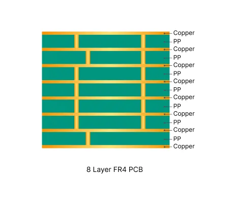
Lamination: Manufacturing 8-layer FR4 PCBs involves greater complexity than lower layer count boards due to multiple lamination cycles, the integration of blind and buried vias, and stricter requirements for dimensional stability and electrical performance. Based on our production experience, several process stages require focused control to ensure consistent quality and yield. Multi-stage Lamination 8-layer boards are typically built using two or three lamination cycles, depending on the stackup design. Each lamination introduces risks related to layer registration, resin flow, and thermal stress. We pay close attention to temperature ramp rates, pressure distribution, and vacuum levels during pressing to minimize voids and delamination. Symmetric copper distribution across the stackup, combined with copper thieving patterns, is applied to reduce warpage caused by repeated thermal cycles.
Drilling: Drilling and Via Processing Drilling operations in 8-layer boards include through holes, blind vias, and buried vias. Blind and buried vias require more precise depth control and specialized desmear processes, particularly when high Tg materials are used. We implement staged drilling strategies and optimize parameters according to via type and material characteristics to maintain hole wall quality and ensure reliable plating adhesion.
Plating: Plating and Metallization Higher layer counts result in increased aspect ratios, making uniform copper deposition inside vias more challenging. Our process focuses on controlling both electroless and electrolytic plating steps to achieve consistent barrel thickness. Regular cross-section analysis is performed to verify plating quality, especially for blind and buried vias where plating defects can be difficult to detect through standard electrical testing.
Surface Finish: Surface Finish Selection and Application ENIG is the predominant surface finish for 8-layer FR4 boards, especially when fine-pitch components or BGAs are present. We adjust nickel and gold thickness based on copper weight, assembly requirements, and shelf-life expectations. For boards with higher copper weights or specific thermal demands, alternative finishes such as Immersion Silver or HASL may be recommended after evaluating solderability and long-term reliability needs.
Manufacturing Order Profile
| Order Quantity | Order Proportion | Estimated Price Level | Typical Lead Time |
|---|---|---|---|
| Prototype (<=30 pcs) | 61% | From $110 | From 4 days |
| Small volume (30-200 pcs) | 26% | From $130 | From 5 days |
| Mass production (>200 pcs) | 13% | From $200 | From 6 days |
Manufacturing Challenges & Process Optimization
Challenge: Layer Registration Control
Multiple lamination cycles increase the difficulty of maintaining accurate layer-to-layer alignment. Misregistration can lead to reduced annular rings, particularly around blind and buried vias, which may compromise via reliability under thermal stress.
We prioritize symmetric stackup designs and apply copper thieving patterns to balance copper distribution across layers. Pinned lamination fixtures and X-ray alignment systems are used to improve registration accuracy. After lamination, X-ray inspection and cross-section analysis are conducted to verify alignment before drilling. These measures have been particularly effective in boards with dense blind via structures.
Design Considerations
Maintaining symmetry in the layer stackup is one of the most effective ways to control warpage in multi-lamination boards. Placing critical signal layers adjacent to reference planes also supports better impedance control and electromagnetic performance. Early definition of a balanced stackup helps minimize issues during subsequent lamination cycles.
The placement and depth of blind and buried vias should be carefully planned to avoid excessive process complexity. Avoiding the positioning of dense routing or large copper areas directly beneath blind via fields can reduce registration risks. Clear via definitions in the design data also help prevent ambiguity during engineering review.
Uneven copper density across layers or within individual layers can affect lamination quality and final board dimensions. Designers are encouraged to apply copper thieving or grid patterns in areas with low copper density. This practice improves pressure distribution during lamination and reduces the likelihood of localized stress or warpage.
For designs requiring controlled impedance, it is important to define target values and reference layers early. Routing impedance traces with minimal interruptions from vias or irregular copper pours helps maintain consistency. Providing sufficient space for trace width adjustments during the engineering phase can prevent delays in production release.