





Typical Specification Range
| Parameter | Typical Range |
|---|---|
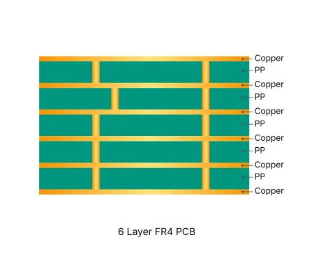
| Layer count | 6 layers |
| Material type | FR4 TG130 to TG170 |
| Surface finish | ENIG, HASL, OSP |
| Thickness | 0.8 mm to 3.0 mm |
| Solder mask | Green, black, red, white, yellow, blue, purple, matte black |
| Copper thickness | 1 oz to 4 oz |
| Special features | Impedance control, blind vias, buried vias, via-in-pad |
Manufacturing Process Insights
Inner Layer Imaging & Etching Multiple cores are imaged and etched with high registration accuracy. Precise annular-ring control and etch-factor compensation on inner layers are essential to maintain impedance and via reliability across the six-layer structure.
Lamination & Stackup Control Cores and prepregs are stacked in a controlled sequence and laminated under heat and pressure. Symmetric copper distribution and dielectric thickness uniformity across all six layers are critical to minimize warpage, ensure layer-to-layer registration, and achieve consistent impedance.
Precision Drilling CNC drilling creates through-holes (and any controlled-depth features) with tight positional tolerance. Higher aspect ratios in 6-layer boards require optimized drill parameters to control hole-wall quality and registration to inner-layer pads.
Desmear & Plating Resin smear is thoroughly removed and electroless copper is deposited, followed by electrolytic plating. Uniform barrel plating through the full board thickness is vital for via reliability under thermal cycling.
Outer Layer Patterning & Etching Outer layers are imaged, plated and etched. Trace compensation and reference-plane integrity are verified to meet controlled-impedance targets common on 6-layer designs.
Solder Mask & Via Treatment Solder mask is applied with accurate registration. Via tenting, resin plugging or open-window decisions are finalized here; conflicts between plugging and mask openings are resolved to protect surface planarity and solderability.
Routing, V-Scoring & Final Inspection Boards are separated by routing or V-scoring. Edge clearance, panelization integrity and copper-to-outline spacing are confirmed. 100% electrical testing and dimensional inspection ensure multilayer continuity and compliance before shipment.
Manufacturing Order Profile
| Order Quantity | Order Proportion | Estimated Price Level | Typical Lead Time |
|---|---|---|---|
| Prototype (<=30 pcs) | 58% | From $30 | From 2 days |
| Small volume (30-200 pcs) | 27% | From $80 | From 2 days |
| Mass production (>200 pcs) | 15% | From $140 | From 3 days |
Manufacturing Challenges & Process Optimization
Stackup Confirmation & Copper Balance / Warpage Control
Customer-supplied stackups frequently deviate from proven 6-layer constructions, creating asymmetric copper distribution or incorrect dielectric thicknesses.
This leads to warpage, registration shift, thickness deviation and unstable impedance — problems that are significantly amplified compared with 2- or 4-layer boards.
✓ Align stackup to a symmetric, process-proven 6-layer configuration while preserving target thickness and impedance.
✓ Enforce balanced copper distribution across all layers.
✓ Verify finished thickness and bow/twist against IPC limits after first-article lamination.
Design Considerations
Provide a complete, symmetric stackup that matches available core and prepreg materials for 6-layer FR4. Design balanced copper distribution across all layers to control warpage and registration. Confirm finished thickness tolerance early, especially for 1.6 mm or thinner constructions.
Define controlled-impedance requirements with clear stackup and trace geometry. Ensure continuous reference planes (or adequate copper pour/stitching) under impedance-critical traces. Size traces according to actual copper weight and expected etch compensation rather than theoretical values.
Explicitly annotate every hole as PTH or NPTH in both the drill file and fabrication notes. When NPTH holes carry surface pads for mechanical support, state this intent clearly so plating sequence can be set correctly. Avoid hybrid features that create plating ambiguity.
Specify via plugging or tenting method for every via group and ensure the solder-mask openings match that treatment exactly. Avoid single-sided openings on resin-plugged vias. Keep silkscreen clear of plugged via areas to prevent resin overflow and planarity problems.