




Typical Specification Range
| Parameter | Typical Range |
|---|---|
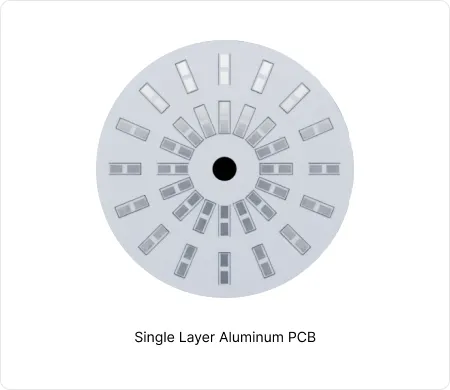
| Layer count | 1 |
| Material type | Aluminum alloy base with dielectric layer |
| Surface finish | HASL, ENIG, OSP |
| Thickness | 0.8mm to 3.2mm |
| Solder mask | White, Black |
| Copper thickness | 1oz to 2oz |
| Special features | High thermal conductivity, exposed aluminum options, selective plating |
Manufacturing Process Insights
Material Preparation and Lamination
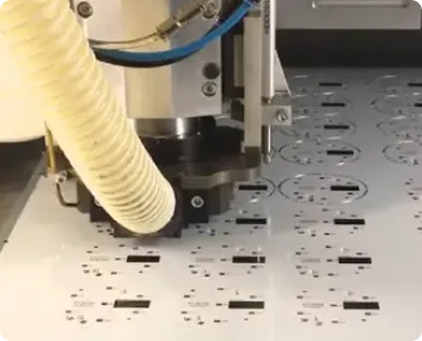
Aluminum sheets are cleaned then bonded with dielectric film and copper foil under controlled heat and pressure.
Patterning and Etching
Photoresist application, exposure, and etching define the circuit pattern on the copper layer.
Drilling and Plating
Precision drilling creates holes. Copper plating follows to establish electrical connections where required.
Surface Finish Application
Finish selection balances solderability, thermal performance, and environmental protection needs.
Process controls manage thermal expansion mismatch to prevent warping during lamination and assembly.
Manufacturing Order Profile
| Order Quantity | Order Proportion | Estimated Price Level | Typical Lead Time |
|---|---|---|---|
| Prototype (<=30 pcs) | 44% | From $1 | From 1 day |
| Small volume (30-200 pcs) | 28% | From $5 | From 1 day |
| Mass production (>200 pcs) | 28% | From $40 | From 1 day |
Manufacturing Challenges & Process Optimization
Warpage During Lamination
Single layer aluminum PCBs tend to warp when subjected to repeated thermal cycles during manufacturing and assembly.
Root cause relates to the mismatch in thermal expansion coefficients between the aluminum base and copper foil under heat and pressure.
Warpage reduces SMT placement accuracy, creates inconsistent solder joints, and lowers long-term reliability in power electronics.
Optimized lamination parameters reduce internal stress.
Engineers apply controlled ramp rates and balanced pressure profiles. Preconditioning of raw materials removes moisture before bonding.
Flatness inspection under thermal stress verifies compliance before release to assembly.
Design Considerations
Define stackup with appropriate dielectric thickness between aluminum base and copper. This controls thermal resistance and electrical isolation. Account for final thickness effects on mechanical stability during reflow.
Limit plated through vias due to the conductive aluminum core. Surface mount technology is preferred. Thermal relief strategies must maintain electrical isolation while supporting heat flow.
Select aluminum alloy according to thermal conductivity and mechanical strength needs. Dielectric choices balance heat transfer with processability. Verify material compatibility with operating environment and assembly temperatures.
Match surface finish to assembly process and product lifecycle. ENIG offers reliable soldering and corrosion resistance. OSP suits cost-driven applications with controlled storage and shorter service life.