Rigid-Flex PCB

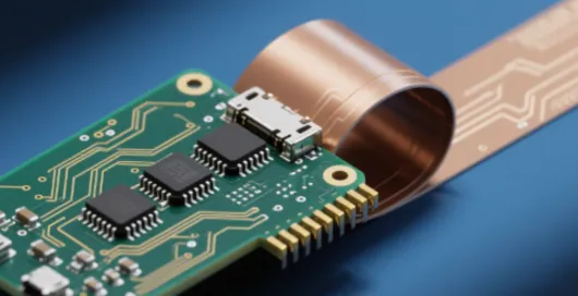
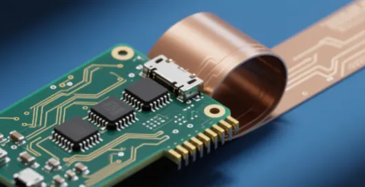
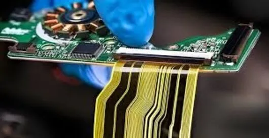
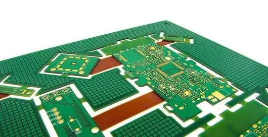
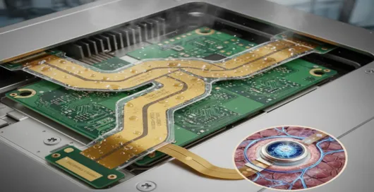
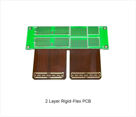
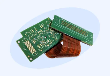
A rigid-flex PCB combines rigid and flexible circuit layers into a single structure, offering both durability and design flexibility. It allows 3D configurations, reduces connectors, and improves reliability. CEZON’s rigid-flex PCBs are ideal for compact, high-performance devices requiring stable signal integrity and mechanical strength.

Learn More About Capabilities

Features of Rigid-Flex PCBs

  • High Space Utilization
  • Excellent Reliability
  • Superior Signal Integrity
  • Outstanding Environmental Adaptability
  • The flexible section of a flex or rigid-flex PCB can be bent, folded, or routed in three dimensions, allowing designers to bypass internal mechanical obstructions and densely packed components. This capability significantly improves internal layout efficiency and reduces the overall product size. For example, in consumer electronics such as smartphones and tablets, using flexible circuits in hinge areas, battery connections, and display modules can reduce device thickness by up to 30%, enabling sleeker and more compact designs. In wearables, flexible PCBs allow electronics to conform to curved surfaces, maximizing space without sacrificing performance.

  • lexible PCBs enhance system reliability by minimizing the number of solder joints, connectors, and wiring harnesses—common failure points in traditional assemblies. Fewer interconnects can reduce the failure rate by up to 50% during long-term operation. Additionally, the integrated structure of flexible circuits provides strong resistance to vibration, impact, and thermal cycling. These advantages make them highly suitable for automotive-grade applications such as in-vehicle sensors, ADAS cameras, dashboard modules, and engine-bay electronic control units, where durability and stability are critical under harsh operating conditions.

  • Fine-pitch traces in the flexible area, often with line width/spacing ≤ 0.1 mm, help minimize signal attenuation and electromagnetic interference. Combined with advanced stack-up design and high-performance materials, flexible PCBs can achieve ±7% impedance control accuracy, ensuring stable signal transmission even at very high frequencies. These characteristics make them ideal for 5G communication infrastructure, high-speed data transmission modules, RF antennas, camera signal lines, and other applications requiring low loss and high-frequency reliability.

  • Flexible PCBs typically use polyimide (PI) substrates, offering exceptional thermal and chemical resistance. PI materials withstand temperatures above 260°C, maintain excellent dimensional stability, and resist corrosion from oils, solvents, and industrial chemicals. When combined with protective surface treatments, such as conformal coatings for dustproof, moisture-proof, and oxidation resistance, flex circuits can reliably operate in harsh environments. They are widely applied in industrial automation equipment (e.g., robots, SMT equipment, high-temperature workshops), aerospace systems, medical implantables, and other devices requiring long-term performance in challenging conditions.

Rigid-Flex PCBs Manufacturing Insights

Rigid-Flex PCB Design Guidelines

1. Material and Stackup Configuration

Select polyimide for flex areas due to its superior flexibility and thermal stability; use epoxy glass for rigid substrates. Prioritize rolled annealed copper in flexible sections to avoid brittleness from electrodeposited copper. Ensure symmetric layer counts in rigid zones and thin flex stacks (1/2–5 mil) for a minimum dynamic bend radius of 100x material thickness. Consult manufacturers early to confirm material compatibility with environmental factors.

2. Bending and Mechanical Layout

Maintain a minimum bend radius of 12–24x circuit thickness, aligning with copper grain direction to prevent cracks; avoid sharp angles. Design gradual transitions between flex and rigid areas, incorporating support pins or connectors for stress relief. For dynamic flexing, add redundant traces; static bends support up to 20 layers. Use 3D software for bend simulation and test under vibration and cycles for reliability.

3. Routing, Vias, and Shielding

Route traces straight and perpendicular in flex zones with 3–5 mil widths, staggering across layers; employ curved corners and teardrops at junctions. Confine vias and through-holes to rigid areas to avoid fractures. Use cross-hatched ground planes instead of solid copper for EMI shielding while preserving flexibility. Place components on rigid sections, optimizing high-frequency signals with blind/buried vias.

4. Components and Manufacturing Best Practices

Avoid components in bend areas, favoring rigid supports for stability; ensure even distribution for double-sided assembly. Adhere to IPC-2223 standards and conduct DFM reviews to optimize panel nesting. Prototype testing in real environments with ±0.002, tolerances is essential. Early collaboration with fabricators can reduce costs by up to 20%.

Rigid-Flex PCBs FAQs

Q1: Why is the cost generally higher than a standard rigid PCB?
A1: The higher cost is due to the increased complexity of the manufacturing process, which involves unique steps like differential etching, complex multi-layer lamination of dissimilar materials, and rigorous testing protocols for both rigid and flexible sections. The specialized flexible materials themselves are also more expensive than standard rigid materials.
Q2: What is the lead time for rigid-flex PCB production?
A2: Lead time depends on complexity and volume—typically 7–15 working days for prototypes and 2–4 weeks for mass production orders.
Q3: What are the advantages of rigid-flex PCBs?
A3:They offer excellent space efficiency, mechanical stability, and design flexibility, reducing the need for connectors and improving signal integrity.

Get in Touch