




HDI PCB
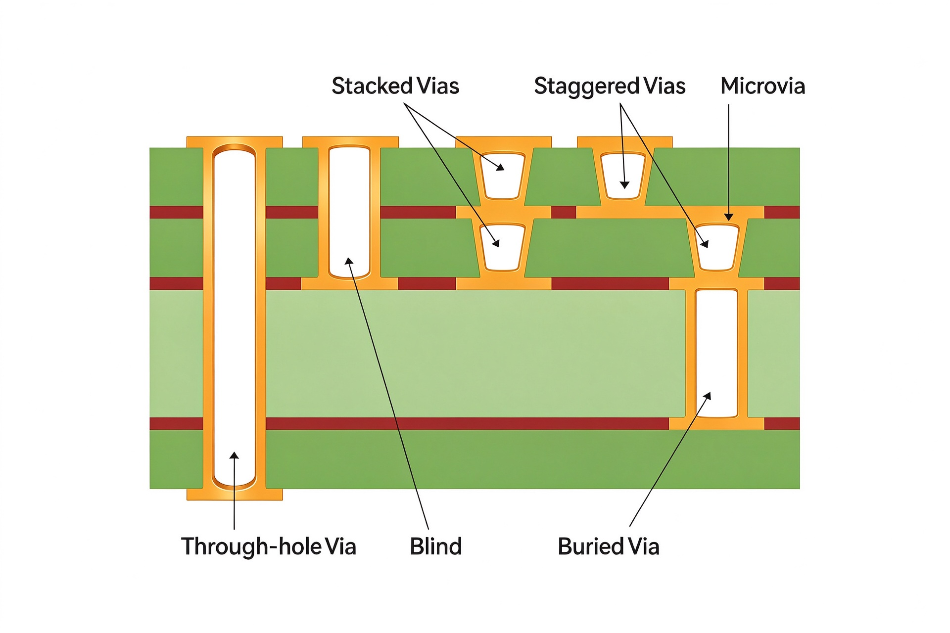
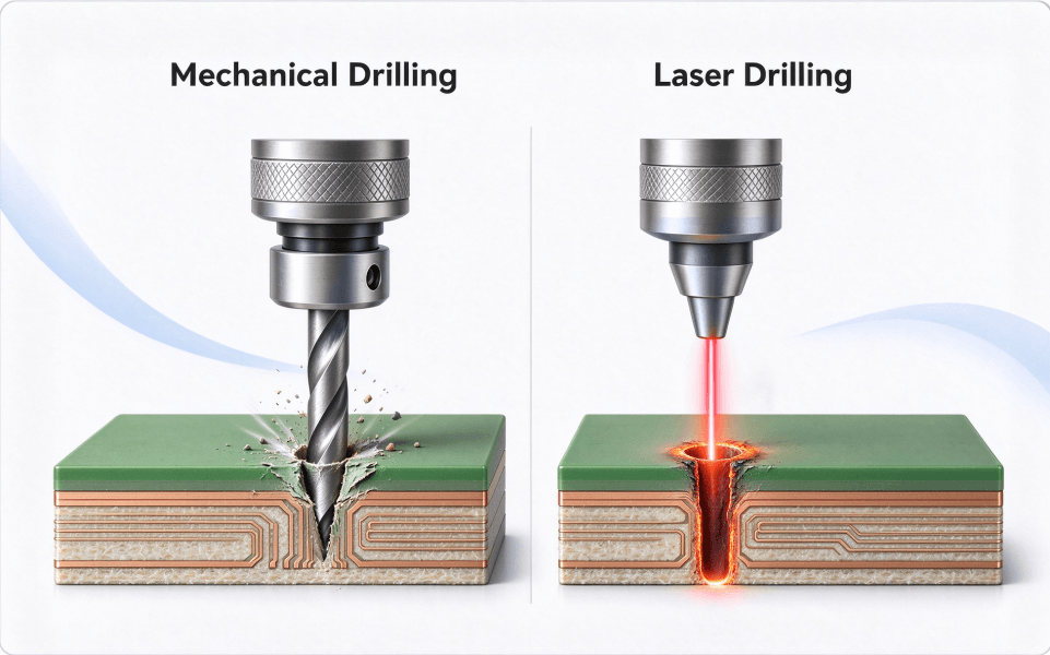
An HDI PCB (High-Density Interconnect) is a board with higher wiring density than a conventional multilayer PCB. It uses laser-drilled microvias, blind and buried vias, and finer lines and spaces — typically ≤100 μm traces and microvias under 150 μm — instead of relying only on mechanically drilled through-holes.
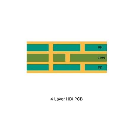
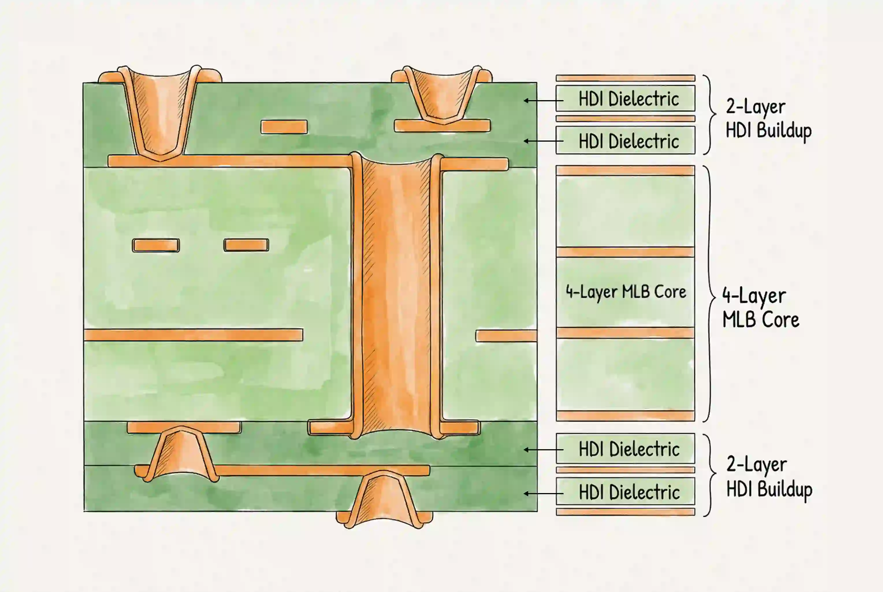
Built as 1+N+1, 2+N+2, or any-layer stack-ups, HDI shortens signal paths and opens routing under fine-pitch BGAs. That is why it shows up in smartphones, 5G modules, automotive controllers, medical devices, and other compact, high-speed products.
| Category | Standard | Sample |
|---|---|---|
| HDI structure | Up to 3+N+3 | Up to 6+N+6 |
| Any-layer interconnect | Yes | Yes |
| Layer count | Up to 16 layers | Up to 20 layers |
| Min. laser blind via | 70 μm | 60 μm |
| Blind-via aspect ratio | 0.8:1 (60–200 μm) | 1:1 |
| Laser hole position accuracy | ≤10 μm | — |
| Layer-to-layer registration | ≤50 μm | ≤50 μm |
| Board thickness | 0.3–3.2 mm | 0.2–3.2 mm |